Solder printing inspection apparatus and solder printing system

a technology of inspection apparatus and solder printing, which is applied in the inspection/indentification of circuits, television systems, instruments, etc., to achieve the effect of suppressing the lowering of productivity

Active Publication Date: 2011-09-08
CKD
View PDF4 Cites 5 Cited by
  • Summary
  • Abstract
  • Description
  • Claims
  • Application Information

AI Technical Summary

Benefits of technology

[0009]In one or more embodiments, the present invention provides a solder printing inspection apparatus an

Problems solved by technology

A solder bridge having a bridge distance exceeding the permissible range in the above-described manner is not a minor solder br

Method used


Image

  • Solder printing inspection apparatus and solder printing system
  • Solder printing inspection apparatus and solder printing system
  • Solder printing inspection apparatus and solder printing system

Examples


Embodiment Construction

[0037]Embodiments of the present invention are explained below, referring to the attached figures. In embodiments of the invention, numerous specific details are set forth in order to provide a more thorough understanding of the invention. However, it will be apparent to one of ordinary skill in the art that the invention may be practiced without these specific details. In other instances, well-known features have not been described in detail to avoid obscuring the invention.

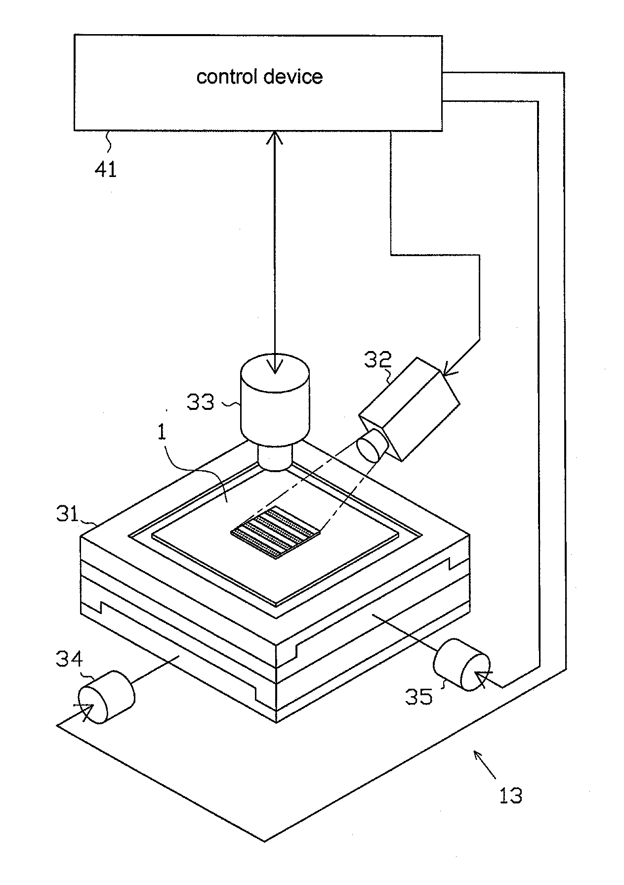
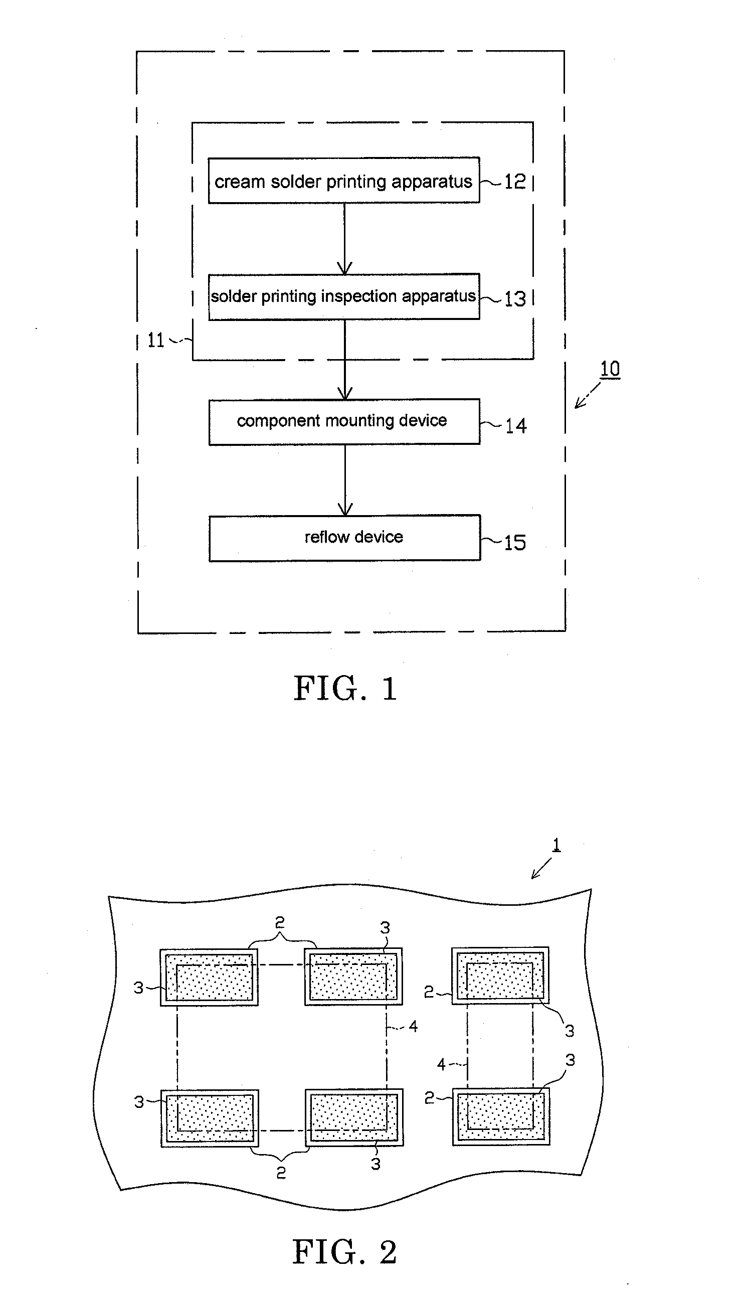
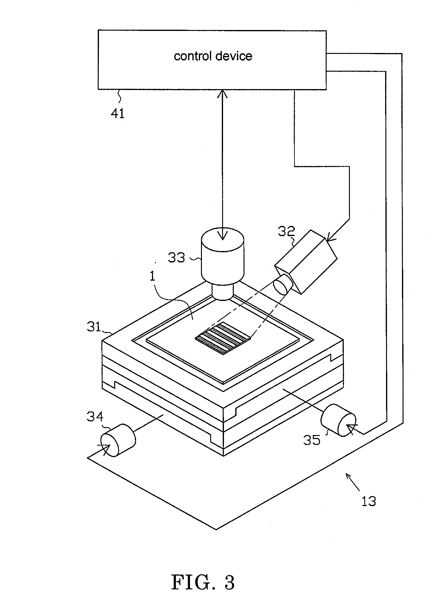
[0038]FIG. 1 is a simplified drawing showing schematically part of the manufacturing line of a printed circuit board according to one or more embodiments of the present invention.

[0039]Firstly, structure of the printed circuit board will be explained. As shown in FIG. 2, a printed circuit board 1 (abbreviated hereinafter as the “circuit board”) has multiple lands 2. In addition to viscous cream solder (abbreviated hereinafter as “solder”) being printed on the land 2, an electronic component 4, such as a chip and...


PUM


Abstract

A solder printing inspection apparatus for inspection of solder printed on a circuit board has a multiplicity of lands for mounting of electronic components. The apparatus includes an irradiation unit for irradiating a light on the circuit board, an imaging unit for imaging the circuit board irradiated by the light, a solder bridge detection unit for detecting a solder bridge connecting two of the lands based on an image data imaged by the imaging unit, a distance calculation unit for calculating a bridge distance as distance between two lands contacting the solder bridge or solder bridging regions or solder detection frames corresponding to the two lands contacting the solder bridge, and a distance determination unit for determination of whether or not the bridge distance is within a permissible range.

Description

CROSS-REFERENCE TO RELATED APPLICATIONS[0001]This application claims priority to Japanese Patent Application No. 2010-46318 filed on Mar. 3, 2010 in Japan.BACKGROUND OF INVENTION[0002]1. Field of the Invention[0003]The present invention generally relates to a solder printing apparatus for inspection of solder printed on a printed circuit board and also relates to a solder printer system equipped with the solder printing apparatus.[0004]2. Background Art[0005]In order to mount electronic components on a printed circuit board, generally cream solder is first printed by a solder printer on multiple lands formed on the printed circuit board. Next, the electronic components are provisionally set on the printed circuit board using the viscosity of this cream solder. Thereafter, the above-described printed circuit board is loaded into a reflow furnace and is subjected to a certain reflow process to perform soldering.[0006]Solder bridges may be formed during this type of soldering, and such...

Claims


Application Information

Patent Timeline
IPC IPC(8): H04N7/18G06K9/00
CPCH04N7/18G06K9/00G06F18/00H05K2203/163H05K1/0269G01N21/95684H05K3/3485
Inventor SHINYAMA, TAKAYUKI
Owner CKD
Why Eureka
Try Eureka