Electronic device and manufacturing method of electronic device

Inactive Publication Date: 2011-09-15
RENESAS ELECTRONICS CORP
View PDF7 Cites 55 Cited by
  • Summary
  • Abstract
  • Description
  • Claims
  • Application Information

AI Technical Summary

Benefits of technology

[0011]According to the manufacturing method of an electronic device of the present invention, warp of a support substrate can be r

Problems solved by technology

However, in such electronic devices, during a heating step, warp may occur in the support substrate due to shrinkage on curing of the insulating resin in the resin interconnection layer, a thermal expansion coefficient difference between the

Method used


Image

  • Electronic device and manufacturing method of electronic device
  • Electronic device and manufacturing method of electronic device
  • Electronic device and manufacturing method of electronic device

Examples


first embodiment

[0033](First Embodiment)

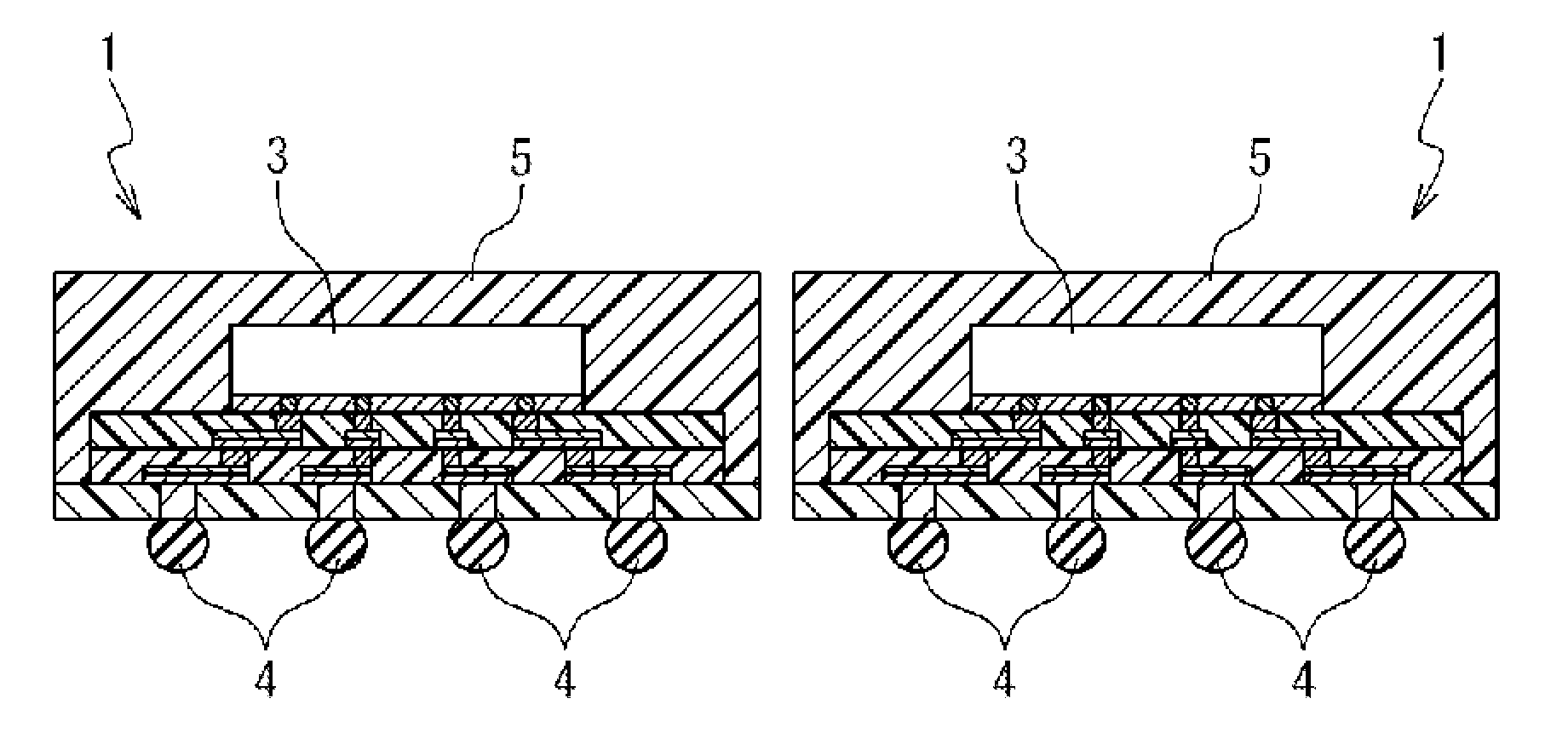
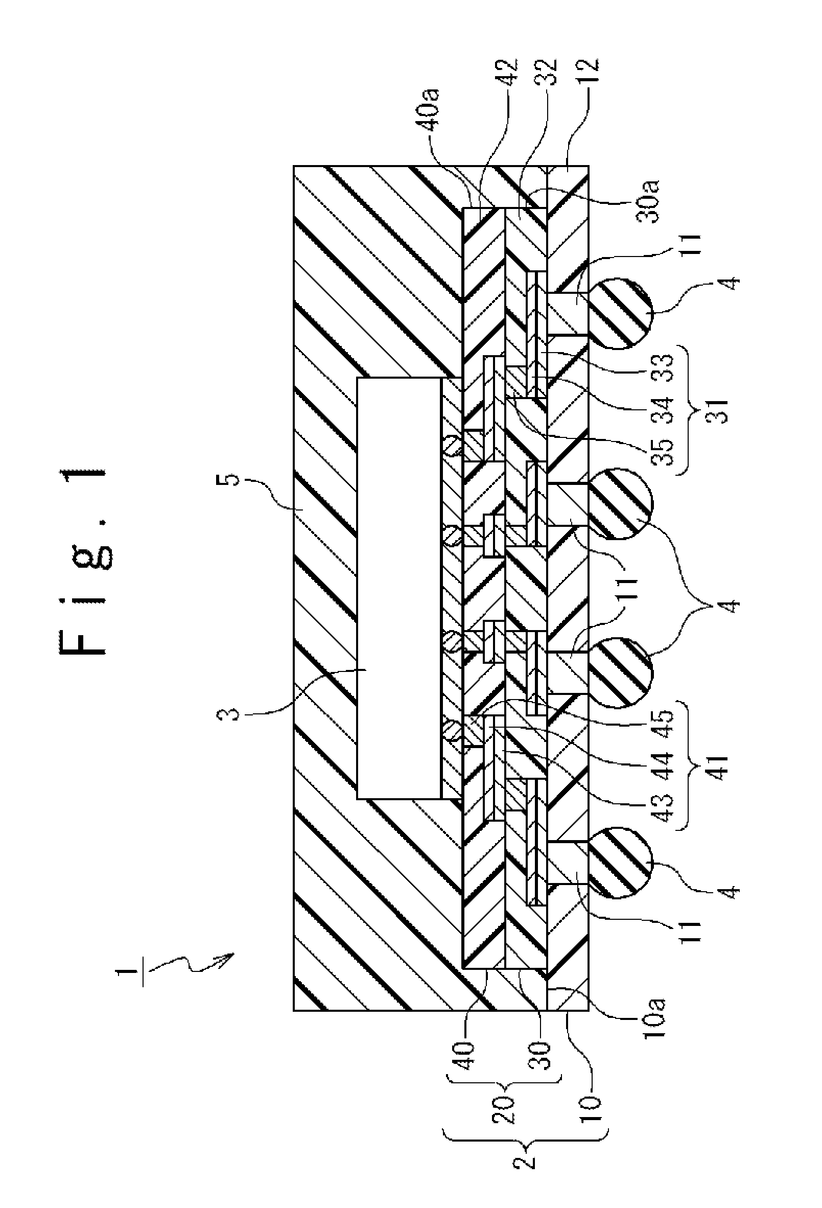
[0034]FIG. 1 is a sectional view of an electronic device 1 according to a first embodiment of the present invention. Referring to FIG. 1, the electronic device 1 includes an interconnection substrate 2, a semiconductor chip 3, a plurality of conductive balls 4 and a mold resin part 5.

[0035]The interconnection substrate 2 is a multilayer interconnection substrate including a lower layer part 10 and a circuit layer part 20. The lower layer part 10 mounts the plurality of conductive balls 4 thereon and is a lowermost layer of the interconnection substrate 2. The lower layer part 10 has a plurality of conductive vias 11 and an insulating part 12. The vias 11 are exposed on an upper surface and a lower surface of the lower layer part 10 and the exposed lower sides each are electrically connected to the conductive ball 4. The insulating part 12 covers the plurality of vias 11 to protect each of the vias 11 so as to expose the vias 11 on the upper surface and the lo...

second embodiment

[0057](Second Embodiment)

[0058]A second embodiment of the present invention will be described. FIG. 14 is a sectional view showing an electronic device 6 according to the second embodiment of the present invention. The same components in the second embodiment as those in the first embodiment are given the same reference numerals. Referring to FIG. 14, the electronic device 6 according to the second embodiment of the present invention includes an interconnection substrate 7, the semiconductor chip 3, the conductive balls 4 and the mold resin part 5.

[0059]Like the interconnection substrate 2 in the first embodiment, the interconnection substrate 7 is a multilayer interconnection substrate and includes the lower layer part 10 and a circuit layer part 21. The lower layer part 10 is the same as that in the first embodiment. The lower layer part 10 mounts the plurality of conductive balls 4 thereon and is a lowermost layer in the interconnection substrate 2. The lower layer part 10 includ...

third embodiment

[0071](Third Embodiment)

[0072]A third embodiment of the present invention will be described. The electronic device 1 according to the first embodiment of the present invention has the interconnection substrate 2 of three-layered structure and the electronic device 6 according to the second embodiment also has the interconnection substrate 7 of three-layered structure. However, the interconnection substrate of the present invention is not limited to the three-layered structure and may be two-layered structure or four or more-layered structure. The third embodiment of the present invention is an embodiment of an interconnection substrate of four-layered structure. FIG. 19 is a sectional view showing an electronic device 8 according to the third embodiment of the present invention. The same component in the third embodiment as those in the first embodiment are given the same reference numerals. Referring to FIG. 19, the electronic device 8 includes an interconnection substrate 9, the s...


PUM


Abstract

In an electronic device having multilayer resin interconnection layers, it is desired to reduce the warp of its support substrate. It is manufactured by: forming a lower layer including a via and a first insulating part on the support substrate; and forming an intermediate layer including a first interconnection and a second insulating part covering the first interconnection on the lower layer. The lower layer is formed by: forming the first insulating part on a first circuit region and a first region surrounding it; and forming the via on the first circuit region. The intermediate layer is formed by: forming the first interconnection on the first circuit region; forming a film of the second insulation part to cover the lower layer; and removing the second insulating part on the first region such that an outer circumferential part of an upper surface of the lower layer part is exposed.

Description

[0001]This Patent Application is based on Japanese Patent Application No. 2010-056019. The disclosure of the Japanese Patent Application is incorporated herein by reference.BACKGROUND OF THE INVENTION[0002]1.Field of the Invention[0003]The present invention relates to an electronic device having a multilayer interconnection substrate and a manufacturing method of an electronic device.[0004]2.Description of Related Art[0005]There is an interconnection substrate called a multi-layer interconnection substrate in which interconnections are laminated to increase the packaging density. In recent years, various investigations are implemented to the multilayer interconnection substrate. For example, Japanese Patent Application Publication JP-A-Heisei 6-244552 discloses a thin-film multilayer interconnection substrate in which insulating thin-film materials are fixedly laminated on an insulating substrate. The thin-film multilayer interconnection substrate is characterized in that insulating...

Claims


Application Information

Patent Timeline
IPC IPC(8): H01L21/84H01L23/48
CPCH01L21/4857H01L2224/0401H01L21/568H01L21/6835H01L23/3121H01L23/3128H01L23/49816H01L23/49822H01L23/49827H01L24/81H01L24/97H01L2221/68345H01L2224/04105H01L2224/16227H01L2224/221H01L2224/73204H01L2224/81005H01L2224/81815H01L2224/8184H01L2224/95001H01L2224/97H01L2924/01013H01L2924/01029H01L2924/01033H01L2924/01046H01L2924/01078H01L2924/01079H01L2924/01082H01L2924/10329H01L2924/15174H01L2924/15311H01L2924/15331H01L21/561H01L2224/16225H01L2924/3511H01L2924/01006H01L2924/01005H01L2224/32225H01L2224/81H01L2924/00012H01L2924/00H01L2924/15787H01L2924/181
Inventor MOTOHASHI, NORIKAZUSOEJIMA, KOUJIKURITA, YOICHIRO
Owner RENESAS ELECTRONICS CORP
Why Eureka
Try Eureka