Antenna pattern frame, case of electronic device and mold for manufacturing the same

a technology for electronic devices and antennas, which is applied in the direction of manufacturing tools, resonant antennas, and protecting materials radiating elements, etc., can solve the problems of increased terminal volume of interior antennas, defective appearance, and exterior antennas that are vulnerable, so as to reduce appearance defects

Inactive Publication Date: 2011-09-15
SAMSUNG ELECTRO MECHANICS CO LTD
View PDF9 Cites 7 Cited by
  • Summary
  • Abstract
  • Description
  • Claims
  • Application Information

AI Technical Summary

Benefits of technology

[0015]An aspect of the present invention also reduces appearance defects by stably fixing an antenna pattern frame to a mold for manufacturing a case of an electronic device when molding the case of the electronic device in which an antenna radiator is embedded.

Problems solved by technology

There have been problems in that the exterior type antenna is vulnerable to external impact and the interior type antenna increases the volume of the terminal.
However, the above-mentioned method requires a process of introducing an injection liquid in an extreme situation such as high temperature and high pressure and when an inner space of the mold that becomes the case of the electronic device is larger than the thickness of the antenna pattern frame disposed in the mold for manufacturing the case of the electronic device, there is a problem in that the antenna pattern frame may be pushed into the mold for manufacturing the case of the electronic device by the high-temperature and high-pressure injection liquid.
As a result, the antenna pattern frame is not fixed to the mold for manufacturing the case of the electronic device by the high-temperature and high-pressure injection liquid, thereby causing a defective appearance, that is, quality defects.

Method used


Image

  • Antenna pattern frame, case of electronic device and mold for manufacturing the same
  • Antenna pattern frame, case of electronic device and mold for manufacturing the same
  • Antenna pattern frame, case of electronic device and mold for manufacturing the same

Examples


Embodiment Construction

[0046]Exemplary embodiments of the present invention will hereinafter be described in detail with reference to the accompanying drawings. However, it should be noted that the spirit of the present invention is not limited to the embodiments set forth herein and those skilled in the art and understanding the present invention could easily accomplish retrogressive inventions or other embodiments included in the spirit of the present invention by the addition, modification, and removal of components within the same spirit; however, those are to be construed as being included in the spirit of the present invention.

[0047]Further, throughout the drawings, the same or similar reference numerals will be used to designate the same components or like components having the same functions in the scope of the similar idea.

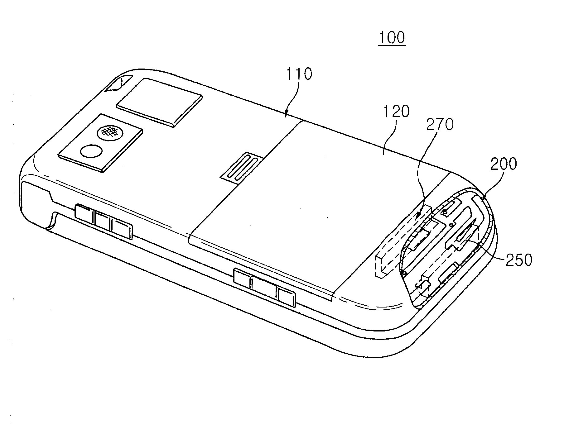
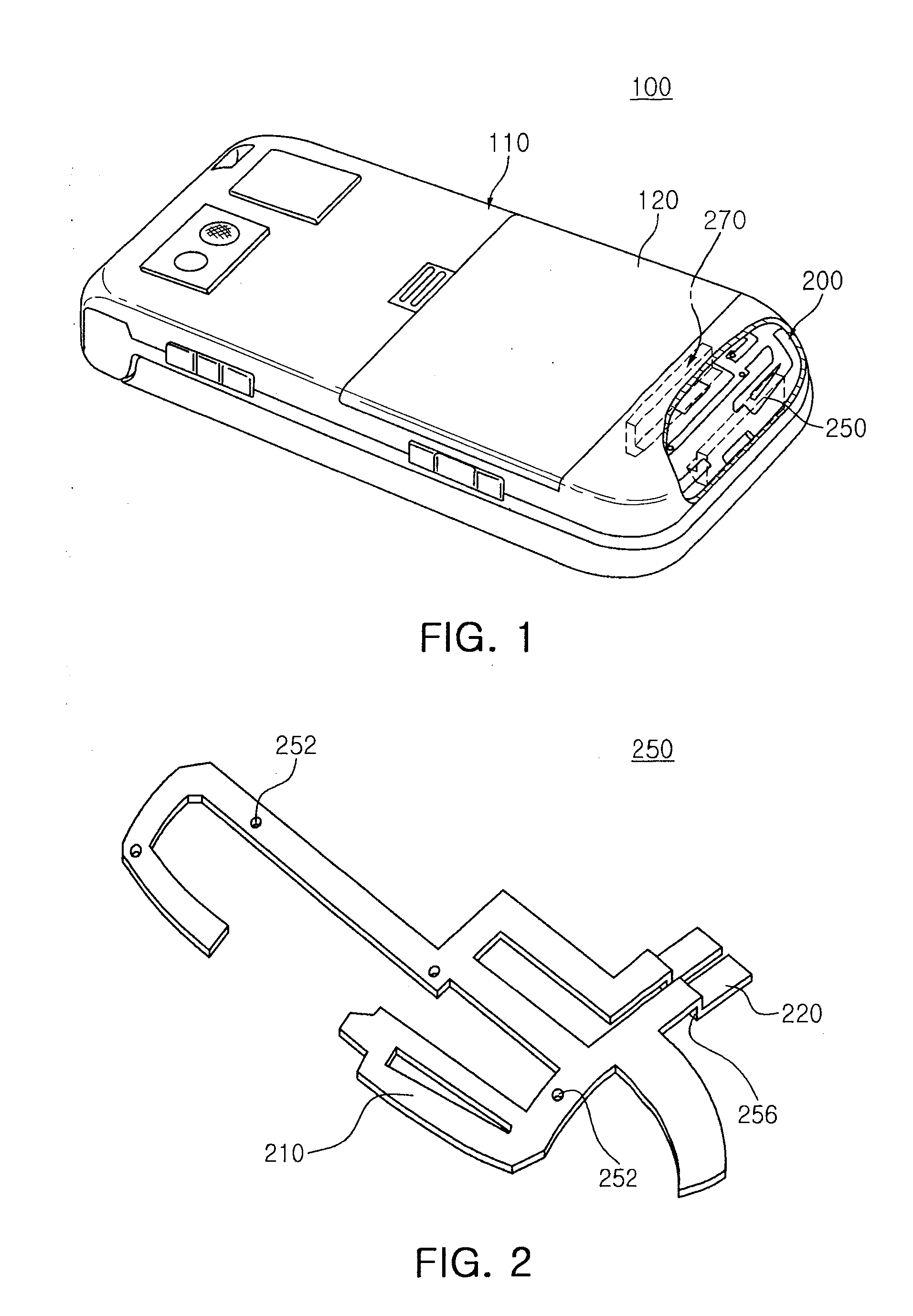
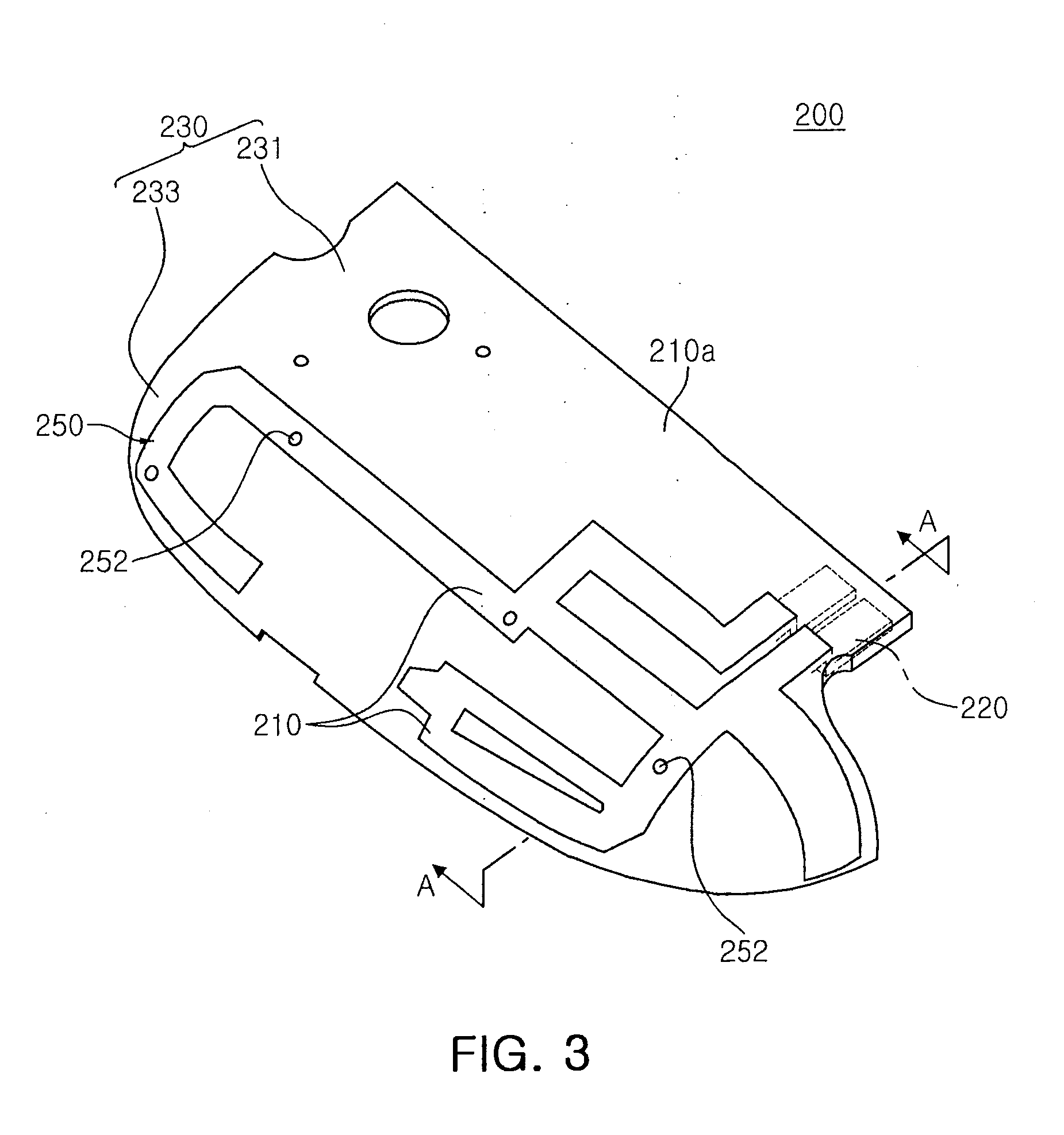
[0048]FIG. 1 is a perspective view schematically showing a partially cutaway case of an electronic device, a mobile communication terminal according to an exemplary embodiment ...


PUM

PropertyMeasurementUnit
bendingaaaaaaaaaa
shapeaaaaaaaaaa
volumeaaaaaaaaaa

Abstract

There is provided an antenna pattern frame according to an exemplary embodiment of the present invention, including: a radiator that includes an antenna pattern part transmitting or receiving signals and a connection terminal part to transmit or receive the signals to and from a circuit substrate of an electronic device; and a radiator frame that supports the radiator, the radiator being manufactured by injection molding and the antenna pattern part being embedded in a case of the electronic device, wherein the radiator frame may be provided with a fastening part to be removed from the manufacturing mold for injection-molding the case of the electronic device in which the radiator is embedded.

Description

CROSS-REFERENCE TO RELATED APPLICATIONS[0001]This application claims the priority of Korean Patent Application No. 10-2010-0022827 filed on Mar. 15, 2010, in the Korean Intellectual Property Office, the disclosure of which is incorporated herein by reference.BACKGROUND OF THE INVENTION[0002]1. Field of the Invention[0003]The present invention relates to an antenna pattern frame, a case of an electronic device, and a mold for manufacturing the same, and more particularly, to an antenna pattern frame having an antenna radiator formed on the surface thereof so that the antenna radiator is embedded in a case of an electronic device, a case of an electronic device, and a mold for manufacturing the same.[0004]2. Description of the Related Art[0005]Mobile communication terminals, for example, cellular phones, PDAs, navigation devices, notebook computers, or the like, that are used to support wireless communication are necessities in modern society. The mobile communication terminals have b...

Claims


Application Information

Patent Timeline
Patent Type & Authority Applications(United States)
IPC IPC(8): H01Q9/04H01Q1/38H01Q1/24B29C45/14
CPCB29C45/006B29C45/14065B29C45/14639B29C45/1671B29C45/4407B29C2045/0093H01Q9/0421B29L2031/3431B29L2031/3437B29L2031/3456B29L2031/3481H01Q1/243H01Q1/40B29C2045/14139
Inventor JEON, DAE SEONGNAM, HYUN KILPARK, HYUN DOLEE, DAE KYUSUNG, JAE SUKBAE, SANG WOO
Owner SAMSUNG ELECTRO MECHANICS CO LTD
Why Eureka
Try Eureka