Integrated Framework for Finite-Element Methods for Package, Device and Circuit Co-Design

a finite element and integrated framework technology, applied in the field of computer-aided design of electronic circuits, to achieve the effect of reducing cost and/or time for the whole (analysis and design plus fabrication)

Inactive Publication Date: 2011-09-15
GLOBALFOUNDRIES INC
View PDF7 Cites 13 Cited by
  • Summary
  • Abstract
  • Description
  • Claims
  • Application Information

AI Technical Summary

Benefits of technology

[0007]greater accuracy in device, circuit, and packaging analysis and design as compared to conventional methods such as the SPICE program;
[0008]reduced number of fabrication cycles due to greater accuracy; and
[0009]even though more computer time may be required for the analysis stage, the overall (analysis and design plus fabrication) cost and / or time are reduced.

Problems solved by technology

Because of device scaling, increased circuit functionalities, and increased chip area, managing the chip temperature is one of the major challenges to optimize the package system and prevent failure of a thermally-stressed area.

Method used


Image

  • Integrated Framework for Finite-Element Methods for Package, Device and Circuit Co-Design
  • Integrated Framework for Finite-Element Methods for Package, Device and Circuit Co-Design
  • Integrated Framework for Finite-Element Methods for Package, Device and Circuit Co-Design

Examples


Embodiment Construction

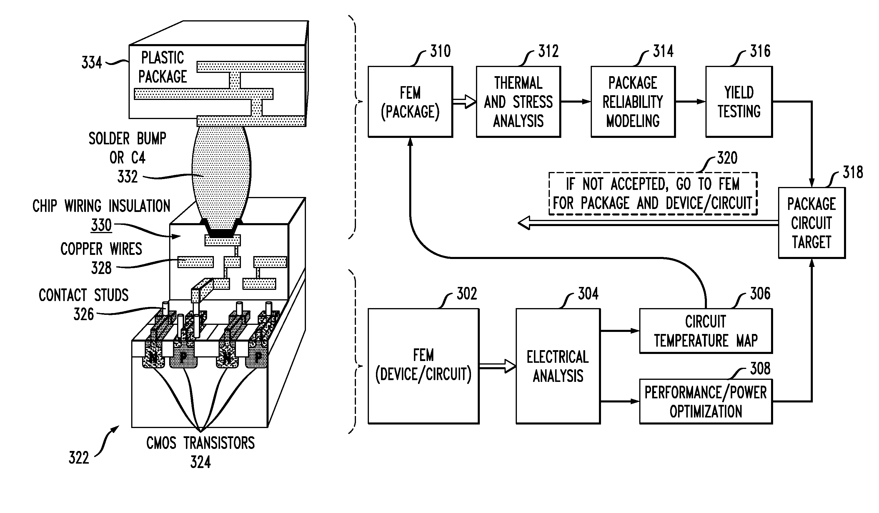
[0020]Because of device scaling, increased circuit functionalities, and increased chip area, managing the chip temperature is one of the major challenges to optimize the package system and prevent the failure of thermally-stressed areas. In accordance with one or more embodiments of the invention, diligent and smart methods using fully-physical and software-based integrated finite-element tools in package, device, and circuit levels can significantly improve package-for-manufacturing by co-optimizing overall chip performance, power, yield, and the package system.

[0021]Current finite element methods include thermal analysis for the package system using mechanical partial differential equations, device design and analysis using electrical and / or physical partial differential equations, and circuit-level analysis by device and / or circuit mix-mode simulations.

[0022]In accordance with one or more embodiments of the invention, integrated finite element methods (also referred to as a frame...


PUM


Abstract

Electrical finite element analysis is carried out on a circuit design, which includes devices, to determine an acceptable power-performance envelope and to obtain data for circuit temperature mapping. A circuit temperature map is developed for the circuit design, based on the data for circuit temperature mapping. Thermo-mechanical finite element analysis is carried out on a package design for the circuit design, based on the circuit temperature map, to determine a package reliability limit based on thermal stress considerations. It is determined whether the package design and the circuit design jointly satisfy: (i) power-performance conditions specified in the acceptable power-performance envelope; and (ii) the package reliability limit based on the thermal stress considerations.

Description

FIELD OF THE INVENTION[0001]The present invention relates to the electrical and electronic and computer arts, and, more particularly, to computer-aided design of electronic circuitry and the like.BACKGROUND OF THE INVENTION[0002]Because of device scaling, increased circuit functionalities, and increased chip area, managing the chip temperature is one of the major challenges to optimize the package system and prevent failure of a thermally-stressed area. Current finite element methods include thermal analysis for the package system using mechanical partial differential equations, device design and analysis using electrical and / or physical partial differential equations, and circuit-level analysis by device and / or circuit mix-mode simulationsSUMMARY OF THE INVENTION[0003]Principles of the invention provide an integrated framework for finite-element methods for package, device and circuit co-design. In one aspect, an exemplary method includes the steps of carrying out electrical finite...

Claims


Application Information

Patent Timeline
Patent Type & Authority Applications(United States)
IPC IPC(8): G06F17/50
CPCG06F17/5018G06F17/5036G06F2217/80G06F2217/78G06F2217/40G06F2113/18G06F2119/08G06F2119/06G06F30/367G06F30/23G06F30/00G06F2117/08G06F2119/12G06F30/398
Inventor KIM, KEUNWOOPARK, SOOJAE
Owner GLOBALFOUNDRIES INC
Why Eureka
Try Eureka