Sacrificial Material to Facilitate Thin Die Attach

a technology of sacrificial material and thin die, which is applied in the direction of semiconductor devices, electrical equipment, semiconductor/solid-state device details, etc., can solve the problems of thin die warpage, poor contact between interconnections, and fragile dies that are difficult to handle during manufacturing processes, and achieve the effect of reducing warpag

Active Publication Date: 2011-09-29
QUALCOMM INC
View PDF21 Cites 14 Cited by
  • Summary
  • Abstract
  • Description
  • Claims
  • Application Information

AI Technical Summary

Benefits of technology

[0010]According to another aspect of the disclosure, an apparatus includes a substrate having a first group of interconnects. The apparatus also includes a die having a second group of interconnects attached to the first group of interconnects. The apparatus further includes means for reducing warpage on a side of the die opposite the second group of interconnects. The warpage reducing means has a sublimation temperature above the liquidus temperature of the second group of interconnects.

Problems solved by technology

Thin dies are fragile and difficult to handle during manufacturing processes.
For example, when heating a thin die during reflow, unbalanced stresses in the die cause the die to warp.
Warpage results in poor contact between interconnects (e.g., non-wets) leading to yield and reliability problems at die thicknesses less than 100 micrometers.
During heating, the die 120 may warp due to unbalanced stresses.

Method used


Image

  • Sacrificial Material to Facilitate Thin Die Attach
  • Sacrificial Material to Facilitate Thin Die Attach
  • Sacrificial Material to Facilitate Thin Die Attach

Examples


Embodiment Construction

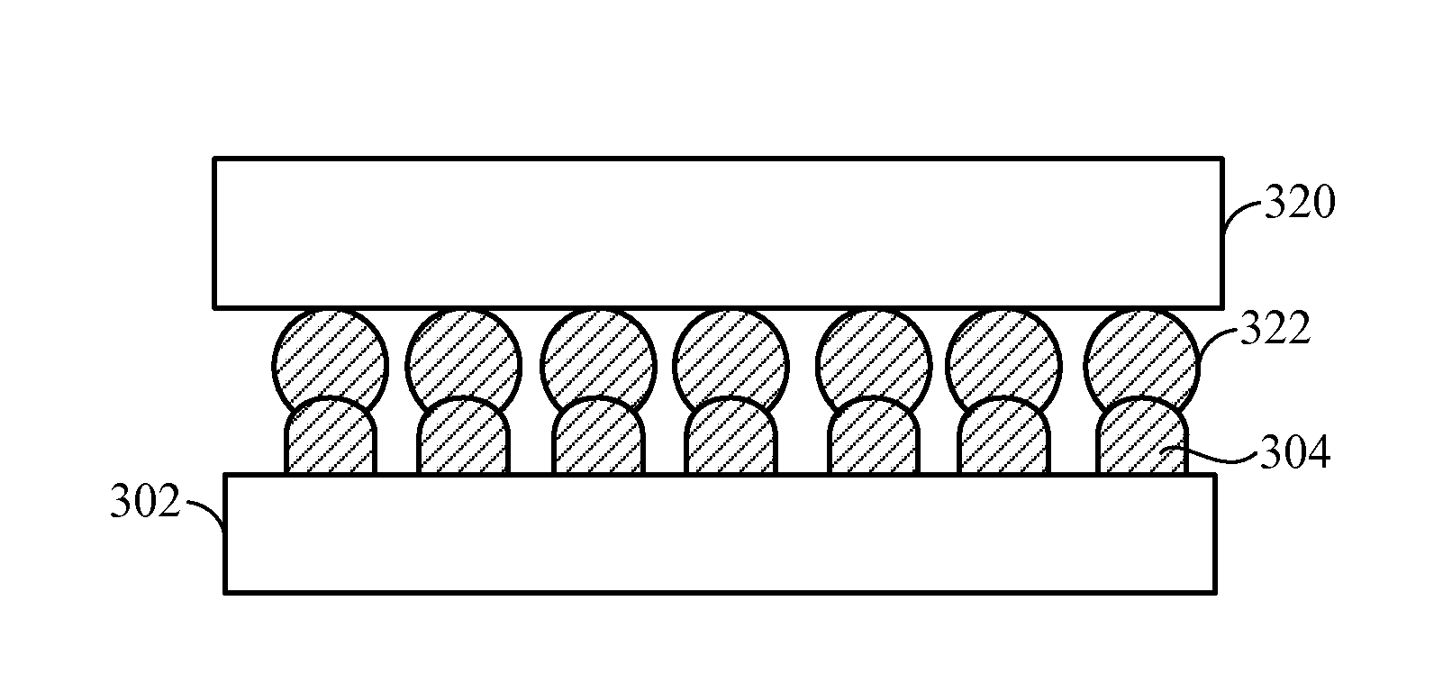
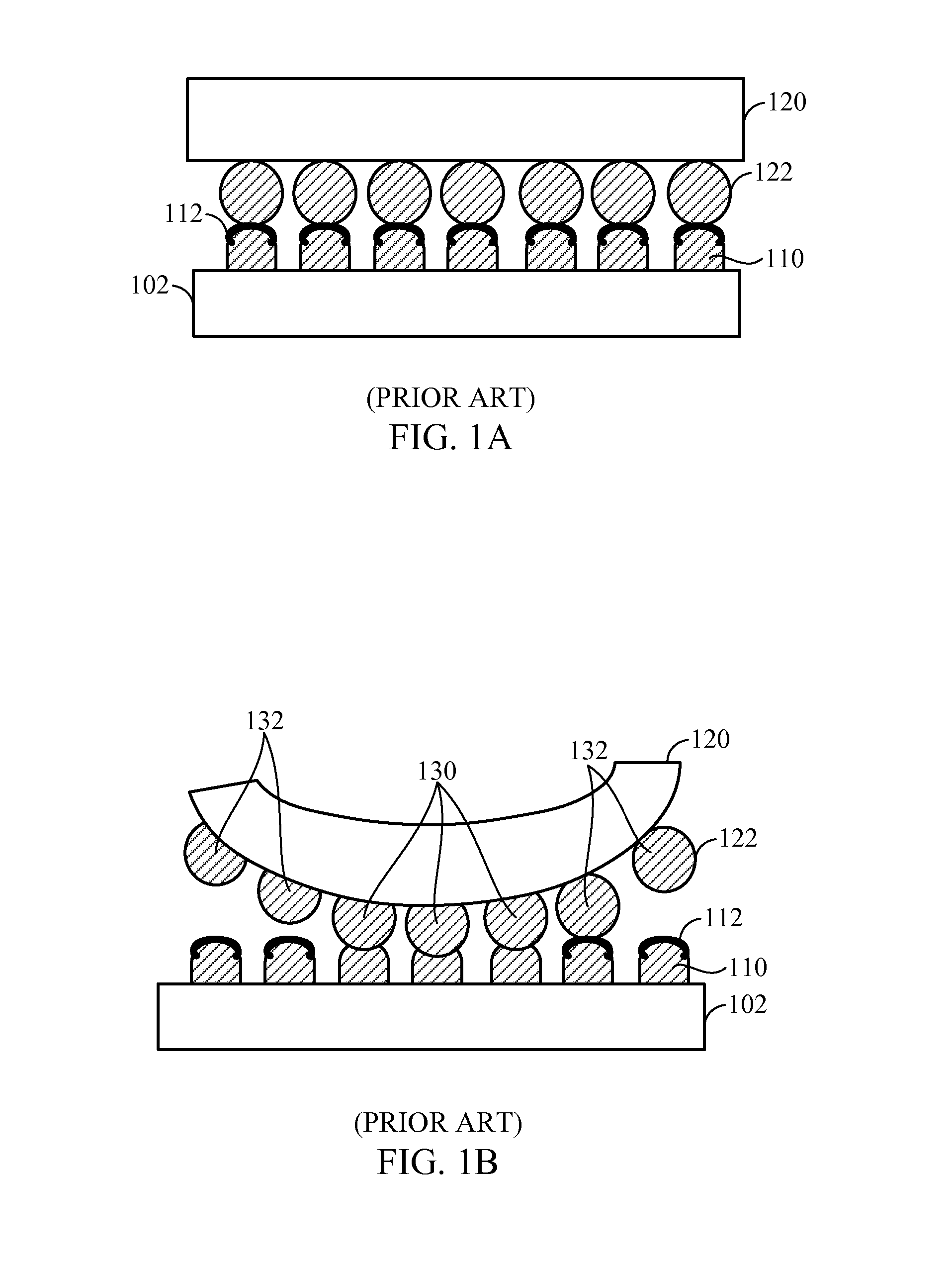
[0025]Depositing a sacrificial material during packaging of an integrated circuit (IC) with a thin die temporarily increases the thickness of the thin die to provide additional support for the die. For example, during solder reflow high temperatures applied to a die may cause warpage of a die having a thickness below 100 micrometers. A sacrificial material may be deposited on the thin die before stacking on a substrate and before application of high temperatures in order to inhibit warpage of the die during reflow. The sacrificial material may be used in packaging techniques such as face-to-face die bonding or other technologies in which contacts of the die are facing the substrate or printed circuit board.

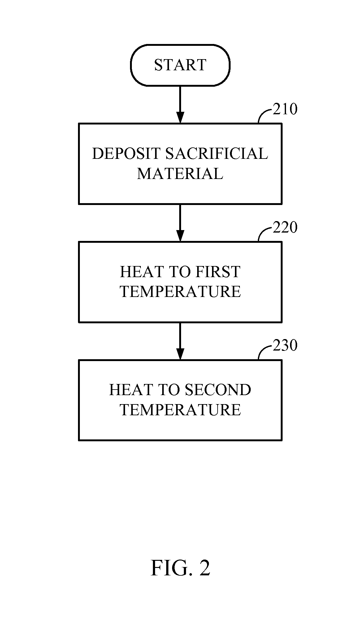
[0026]FIG. 2 is a flow chart illustrating an exemplary process flow for die attach with thin dies according to one embodiment. An exemplary process for die attach begins at block 210 with depositing sacrificial material. FIG. 3A is a cross-sectional view illustrating an exemplary ...


PUM

PropertyMeasurementUnit
thicknessesaaaaaaaaaa
thicknessaaaaaaaaaa
thicknessaaaaaaaaaa

Abstract

A sacrificial material applied to a thin die prior to die attach provides stability to the thin die and inhibits warpage of the thin die as heat is applied to the die and substrate during die attach. The sacrificial material may be a material that sublimates at a temperature near the reflow temperature of interconnects on the thin die. A die attach process deposits the sacrificial material on the die, attaches the die to a substrate, and applies a first temperature to reflow the interconnects. At the first temperature, the sacrificial material maintains substantially the same thickness. A second temperature is applied to sublimate the sacrificial material leaving a clean surface for the later packaging processes. Examples of the sacrificial material include polypropylene carbonate and polyethylene carbonate.

Description

TECHNICAL FIELD[0001]The present disclosure generally relates to integrated circuits. More specifically, the present disclosure relates to packaging integrated circuits.BACKGROUND[0002]Electronic devices are continually shrinking in size to improve portability of the electronic devices. For example, cellular telephones have recently decreased in size to fit in shirt pockets, and are continuing to decrease in size. As the devices shrink, the components inside the device, including the integrated circuits, also shrink. In integrated circuits, a significant amount of the overall thickness is the die rather than circuitry on the die. One method of decreasing the integrated circuit thickness uses thinner dies for the integrated circuits.[0003]Thin dies are fragile and difficult to handle during manufacturing processes. For example, when heating a thin die during reflow, unbalanced stresses in the die cause the die to warp. Warpage results in poor contact between interconnects (e.g., non-...

Claims


Application Information

Patent Timeline
Patent Type & Authority Applications(United States)
IPC IPC(8): H01L23/52H01L21/50
CPCH01L24/13H01L2224/81011H01L24/81H01L25/0657H01L25/50H01L2221/68381H01L2224/81001H01L2224/81193H01L2224/81211H01L2224/81801H01L2225/06513H01L2225/06541H01L2924/01057H01L2924/01082H01L2924/14H01L2924/1433H01L2924/3511H01L2924/01006H01L2924/01033H01L2924/01075H01L2924/01322H01L2924/014H01L24/16
Inventor BCHIR, OMAR
Owner QUALCOMM INC
Why Eureka
Try Eureka