Voltage converter

a voltage converter and converter technology, applied in the field of voltage converters, can solve the problems of high-frequency noise generation, no countermeasures have been taken against high-frequency noise in the modules, and problems in the operation of surrounding devices, so as to reduce the output-side electrical impedance, effectively suppress and block high-frequency noise, and reduce the effect of output-side electrical impedan

Active Publication Date: 2011-09-29
TDK CORPARATION
View PDF4 Cites 27 Cited by
  • Summary
  • Abstract
  • Description
  • Claims
  • Application Information

AI Technical Summary

Benefits of technology

[0018]The invention has been made in view of the problems, and an object of the present invention is to provide a voltage converter capable of reliably preventing malfunctions of an electronic circuit to stably maintain an accurate operation by suppressing high-frequency noise generated on an input side.

Problems solved by technology

However, although the occurrence of the shoot-through current can be prevented by controlling the switching timings in such a manner, another problem may be caused.
As a result, high-frequency noise is generated (however, the generation mechanism is not limited to this).
The high-frequency noise generated by such a mechanism is radiated (unnecessarily radiated) to the outside, and such spurious radiation may cause problems in the operation of surrounding devices or communication jamming between the surrounding devices and may propagate through a floating capacitance of the inductor L or the ground to appear in the output voltage.
However, at present, substantially no countermeasures have been taken against the high-frequency noise in the modules mounting the voltage converter of the related art.
In addition, the use of a configuration in which electrical connection positions between the components of a voltage converter are decreased further, or a wire-to-wire distance is decreased further is generally difficult from the perspective of designing a wiring substrate on which the voltage converter is mounted.
Moreover, even when such a design is employed, there is a possibility that it may increase various other noise components including high-frequency noise.

Method used


Image

  • Voltage converter
  • Voltage converter
  • Voltage converter

Examples


first embodiment

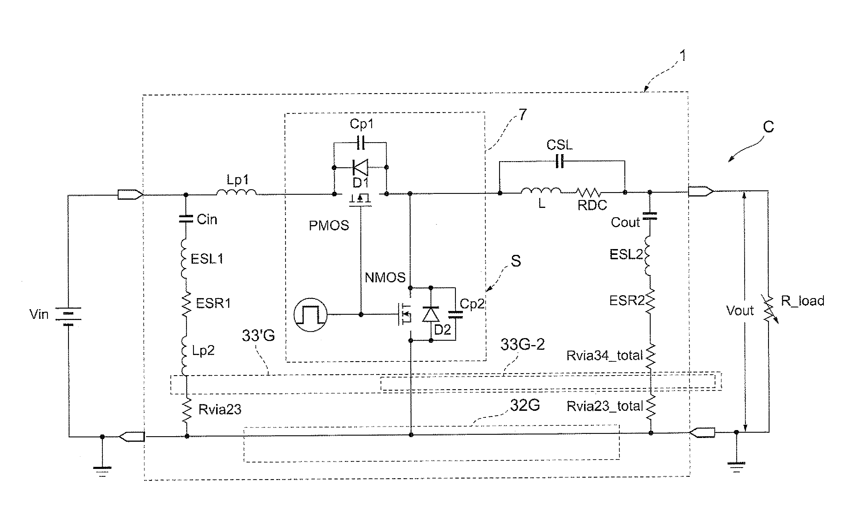
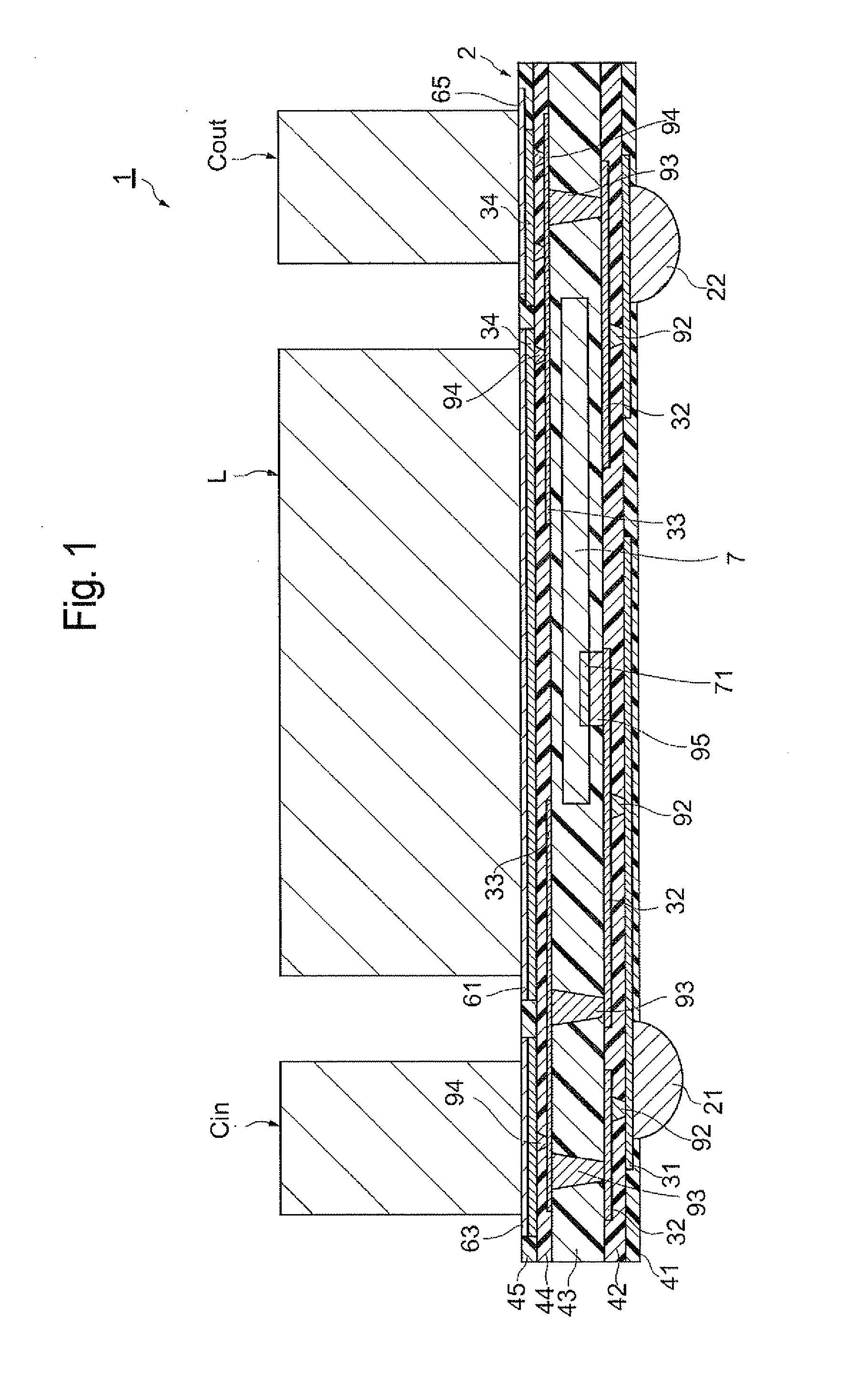
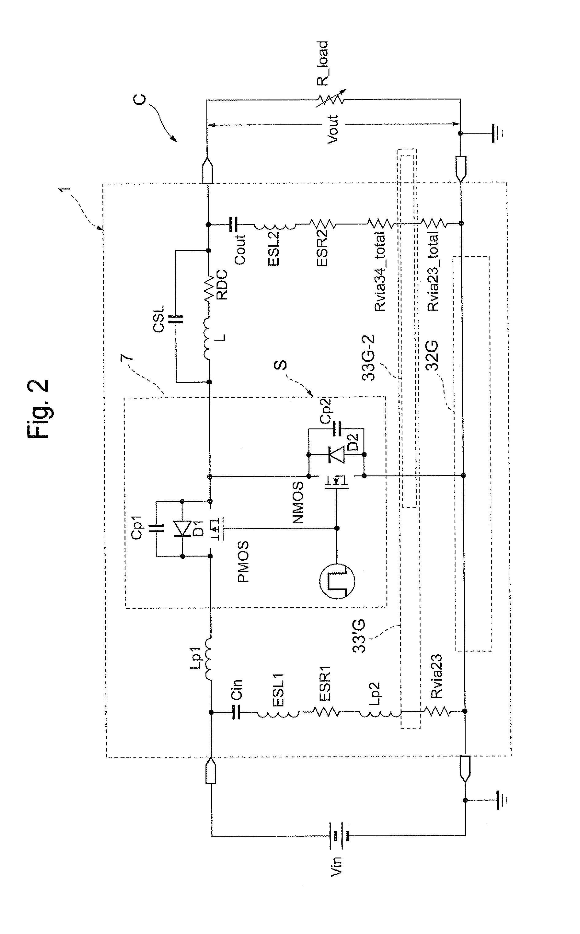
[0049]FIG. 1 is a cross-sectional view schematically showing a structure of a DC-DC converter (power supply module) 1 which is a preferred embodiment of a voltage converter according to the invention. The cross section shows a state in which the DC-DC converter 1 is divided at the position of an IC chip 7 described later and is seen from one side of the IC chip 7. FIG. 2 is an equivalent circuit diagram (including parasitic components) of the DC-DC converter 1 shown in FIG. 1.

[0050]The DC-DC converter 1 includes an active component embedded substrate (substrate) 2, an inductor (passive component) L connected to bonding regions (electrode pads) 61 and 62 of the active component embedded substrate 2, an input-side capacitor Cin connected to bonding regions (electrode pads) 63 and 64 of the active component embedded substrate 2, and an output-side capacitor Cout connected to bonding regions (electrode pads) 65 and 66 of the active component embedded substrate 2. An IC chip 7, for examp...


PUM


Abstract

There is provided a voltage converter capable of reliably preventing malfunctions of an electronic circuit to stably maintain an accurate operation by suppressing high-frequency noise generated on an input side. A DC-DC converter 1 as a voltage converter includes an active component embedded substrate 2 having an IC chip 7 and an input-side capacitor Cin and an output-side capacitor Cout mounted thereon, and ground layers 33G-1 and 33G-2 and a ground layer 32G are formed therein so as to interpose the IC chip 7 therebetween. The input-side capacitor Cin is connected to the ground layer 33G-1, and the output-side capacitor Cout is connected to the ground layer 33G-2. Moreover, the ground layer 32G is connected to the terminals of the IC chip 7, and the input-side capacitor Cin and the output-side capacitor Cout are connected to each other by the ground layers 33G-1 and 33G-2.

Description

CROSS-REFERENCES TO RELATED APPLICATIONS[0001]The present application relates to and claims priority from Japanese Patent Application No. 2010-073129, filed on Mar. 26, 2010, the entire disclosure of which is incorporated herein by reference.BACKGROUND OF THE INVENTION[0002]1. Field of the Invention[0003]The invention relates to a voltage converter in which active components are embedded in (incorporated in, built in) a substrate.[0004]2. Description of the Related Art[0005]A non-insulated step-down DC-DC converter is an example of a voltage converter which is used in an active component mounted on an electronic device. FIG. 20 shows a configuration of a basic circuit of such a non-insulated step-down DC-DC converter. Here, when it is assumed that the input voltage of the non-insulated step-down DC-DC converter is Vin, the output voltage thereof is Vout, and the load resistance thereof is Rload, the state equation of this circuit is expressed by Equation 1 below.[Equation1](tiouttVo...

Claims


Application Information

Patent Timeline
Patent Type & Authority Applications(United States)
IPC IPC(8): G05F3/02
CPCH01L23/50H05K2201/10053H01L24/24H01L2224/24226H01L2924/01029H01L2924/01082H02M3/00H05K1/185H05K2203/1469H01L2924/01006H01L2924/01023H01L2924/01033H01L2924/014H01L2924/13091H05K1/0215H05K2201/1003H01L23/5389H01L2224/04105H01L2224/73267H01L2924/14H01L2223/6677H02M3/003H01L2924/00
Inventor CHIBA, HIRONORI
Owner TDK CORPARATION
Why Eureka
Try Eureka