

Field effect transistor, method of manufacturing field effect transistor, and method of forming groove
- Summary
- Abstract
- Description
- Claims
- Application Information
AI Technical Summary
Benefits of technology
Problems solved by technology
Method used
Image

Examples
Embodiment Construction
[0023]Hereinafter, exemplary embodiments of a field effect transistor, a method of manufacturing the field effect transistor, and a method of forming a groove according to the present invention will be described in detail with reference to the attached drawings. The present invention is not limited to these embodiments but various kinds of modifications are possible without departing from the scope of the invention.
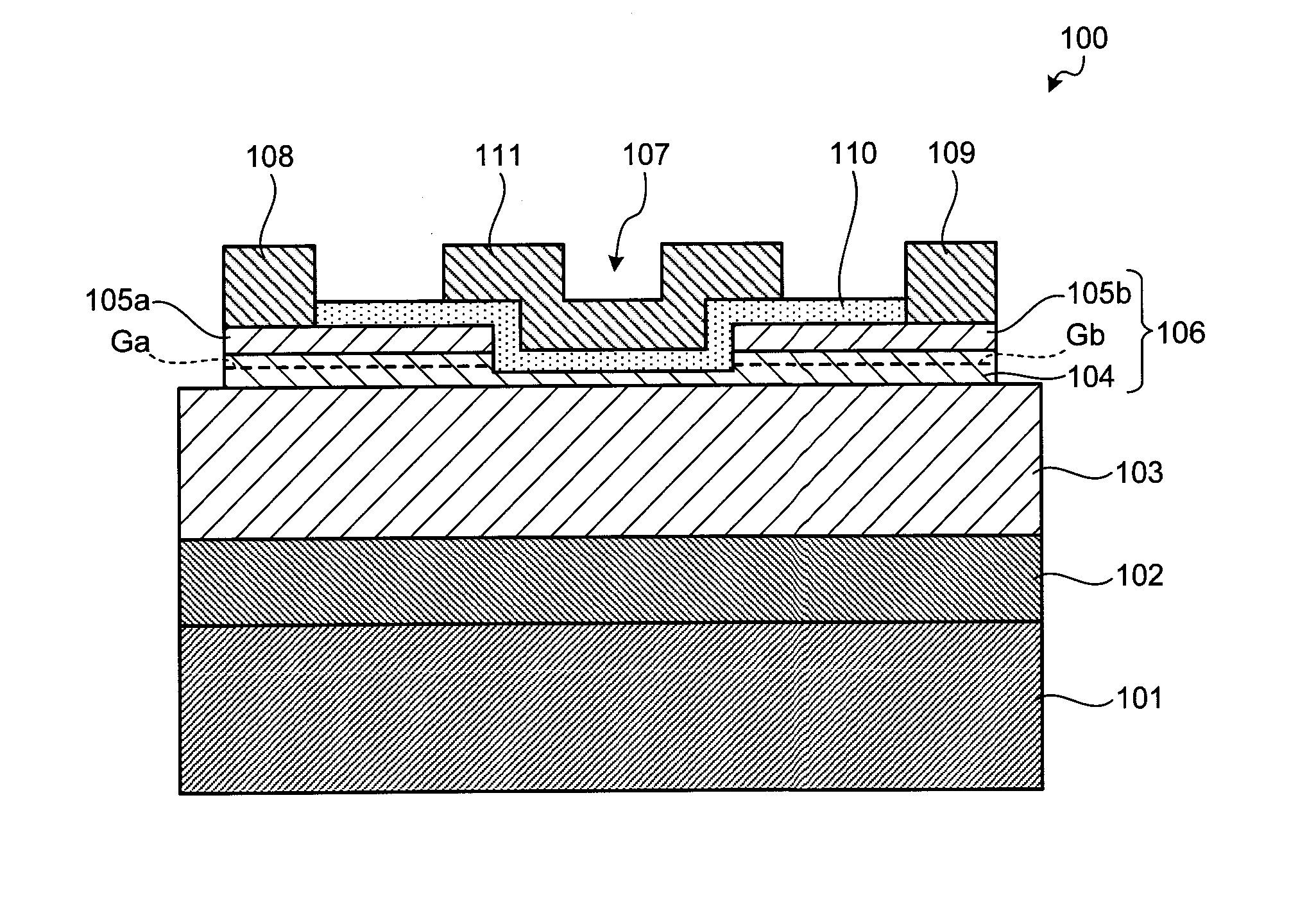
[0024]FIG. 1 is a schematic cross-sectional view of MOSFET 100 according to the first embodiment of the present invention. The MOSFET 100 includes a buffer layer 102, a high resistance layer 103, a channel layer 104, and carrier supplying layers 105a and 105b, on a substrate 101 that is formed of Si and of which the main surface is the surface (111). The buffer layer 102 is formed in a laminated structure of AlN / GaN. The high resistance layer 103 is formed on the buffer layer 102. The channel layer 104 is formed on the high resistance layer 103. The carrier supplying laye...
PUM
 Abstract
Description
Claims
Application Information