Programming at Least One Multi-Level Phase Change Memory Cell

Inactive Publication Date: 2011-10-06
IBM CORP
4 Cites 19 Cited by

AI-Extracted Technical Summary

Problems solved by technology

Storing multiple resistance levels in a PCM cell is a challenging task.
Issues like process variability, as well as intra-cell and ...

Method used

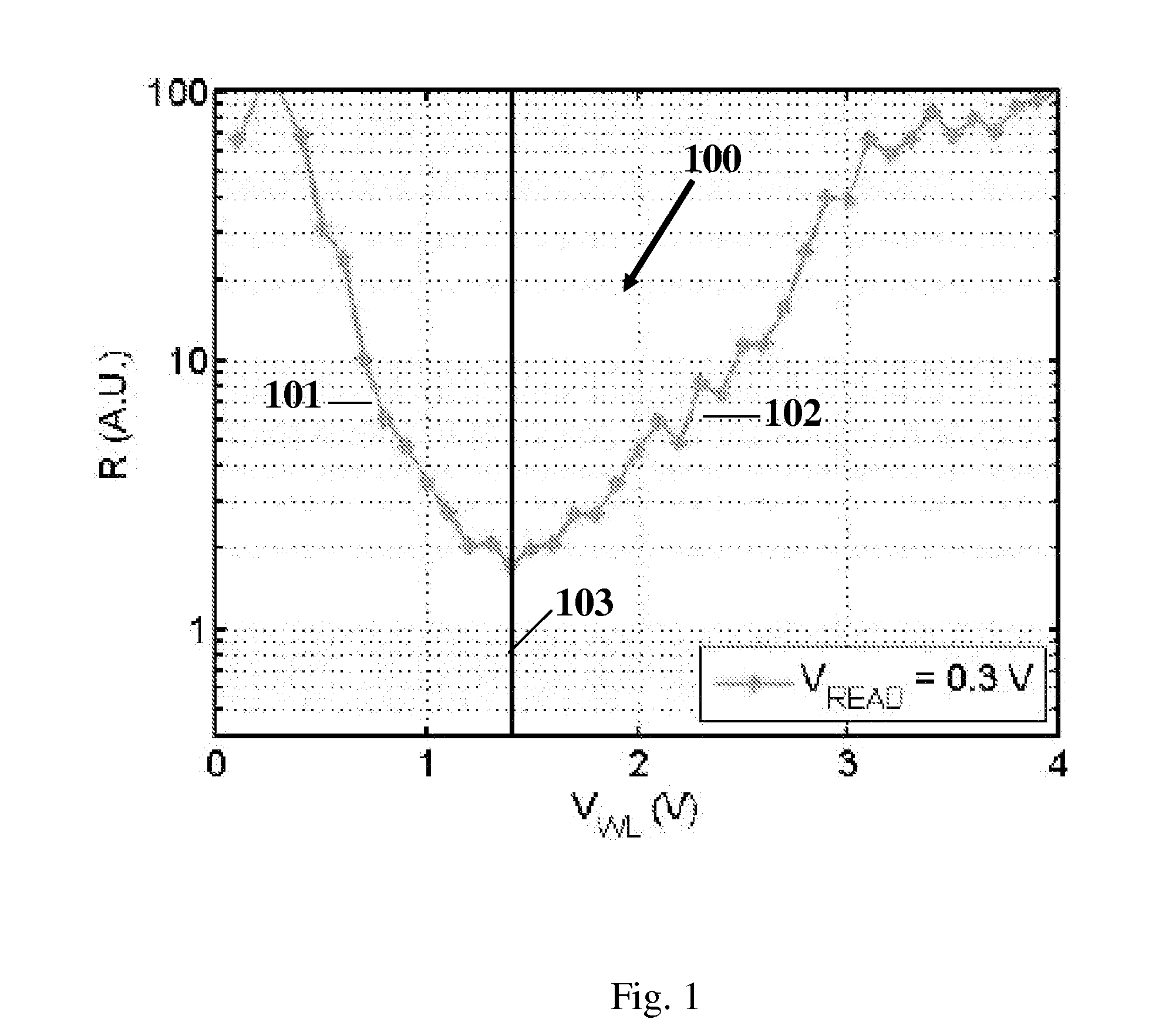
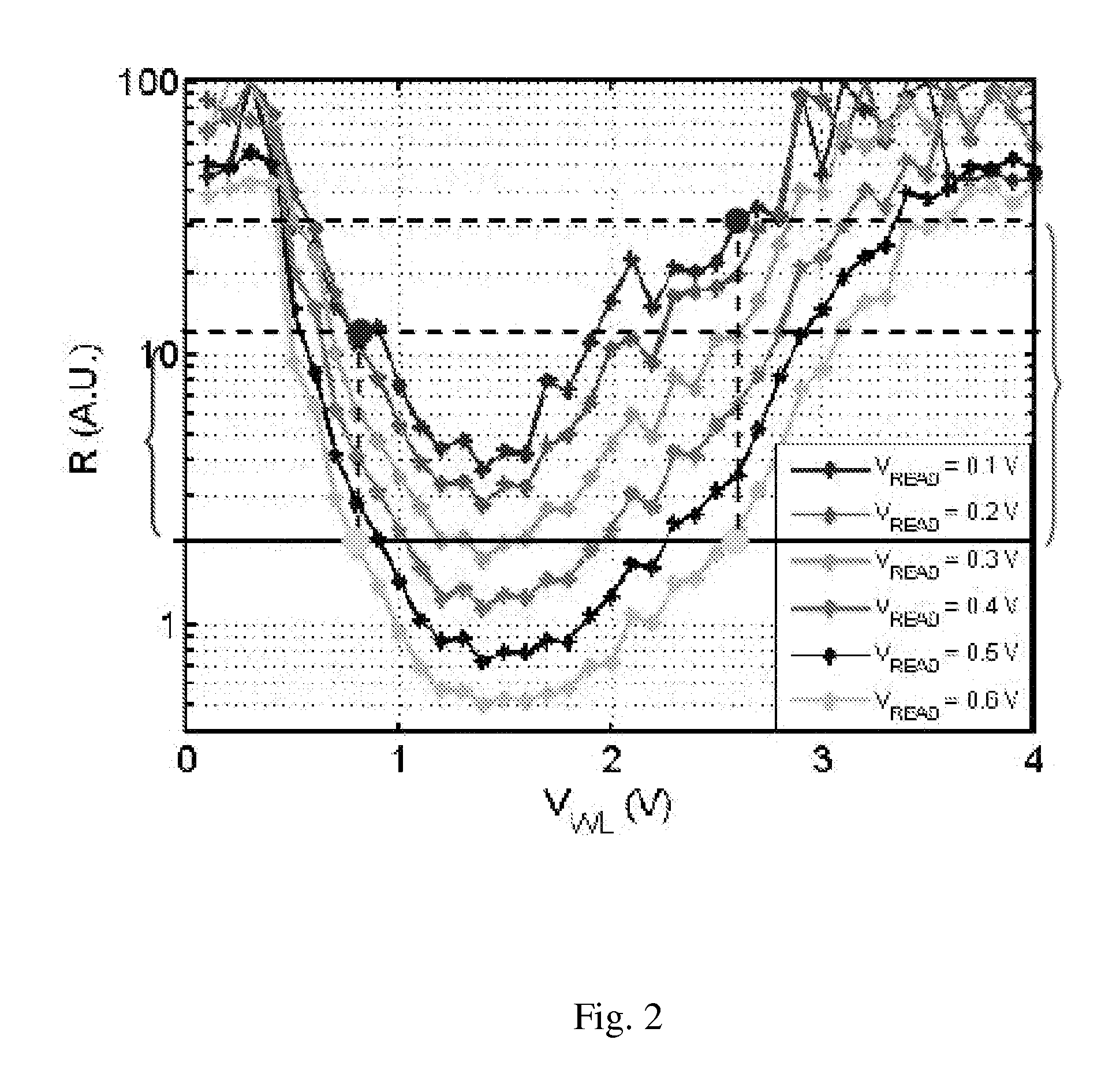
[0073]The present invention may be applied to multi-level Phase Change Memory (PCM) cells. Multi-level functionality, i.e. multiple bits per PCM cell, is a prominent way to increase the capacity and thereby to reduce costs. A multi-level PCM cell is based on storing multiple resistance levels between a lowest (SET) and a highest (RESET) resistance value. The multi...

Benefits of technology

[0018]Thus, the two-dimensional programming scheme according to embodiments of the invention may increase the storage capacity of the PCM cell, since two information entities or levels may be programmed in the same resistance value.
[0019]Therefore, the two-dimensional programming scheme according to embodiments of the invention may have the advantage that the storage levels of the PCM cell may be increased and thus more bits may be stored in one PCM cell.
[0020]Part...

Abstract

A method of applying at least one programming pulse to the a PCM cell for programming the PCM cell to have a respective definite cell state, the definite cell state being defined by a definite resistance level using an annealing pulse or a melting pulse. The respective definite cell state represents two information entities, a step of applying a first reading pulse to the respective programmed PCM cell to provide a first resistance value, a step of applying at least a second reading pulse to the respective programmed PCM cell to provide a second resistance value, the first reading pulse and the second reading pulse being different pulses; and a step of determining the respective definite cell state of the respective programmed PCM cell dependent on the respective provided first resistance value and the respective provided second resistance value.

Application Domain

Digital storage

Technology Topic

PhysicsCell state +1

Image

  • Programming at Least One Multi-Level Phase Change Memory Cell
  • Programming at Least One Multi-Level Phase Change Memory Cell
  • Programming at Least One Multi-Level Phase Change Memory Cell

Examples

  • Experimental program(2)

Example

[0097]Moreover, FIG. 12 shows a block diagram of a first embodiment of a device 10 for programming at least one multi-level PCM cell. Said device 10 has first means 11, second means 12, third means 13 and fourth means 14.
[0098]Said first means 11 are configured to apply at least one programming pulse to the at least one PCM cell for programming said respective PCM cell to have a respective definite cell state. The definite cell state may be defined by a definite resistance level and a type of the at least one applied programming pulse being an annealing pulse or a melting pulse, the respective definite cell state representing two information entities.
[0099]Further, said second means 12 are adapted to apply a first reading pulse to the respective programmed PCM cell to provide a first resistance value.
[0100]Said third means 13 are adapted to apply at least a second reading pulse to the respective programmed PCM cell to provide a second resistance value. The first reading pulse and the second reading pulse are different pulses or reading pulses.
[0101]Said fourth means 14 are adapted to determine the respective definite cell state of the respective programmed PCM cell dependent on the respective provided first resistance value and the respective provided second resistance value or the respective provided current versus reading-pulse amplitude curve.

Example

[0102]FIG. 13 shows a block diagram of a second embodiment of the device for programming at least one multi-level PCM cell. The second embodiment of FIG. 13 includes all features of said first means 11, said second means 12, and said third means 13 and embodies the fourth means 14.
[0103]In particular, said fourth means 14 may be adapted to determine the resistance level and the phase distribution of the programmed PCM cell dependent on the respective provided first resistance value and either the respective provided second resistance value or the respective provided current versus reading-pulse amplitude curve
[0104]Particularly, said fourth means 14 may comprise first providing means 141, second providing means 142 and identifying means 143. The first providing means 141 may be adapted to provide a threshold value. The threshold value may be different depending on the definite resistance level. Furthermore, said second providing means 142 are adapted to provide a measure being the difference between the first resistance value and the second resistance value. Moreover, said identifying means 143 may be adapted to identify the applied programming pulse as a melting pulse, if the respective provided measure is greater than the provided threshold value, or as an annealing pulse, if the respective provided measure is less than the provided threshold value.
[0105]Further, said second providing means 142 and said identifying means 143 may be embodied alternatively. In this regard, said second providing means 142 may be adapted to provide a measure being the slope of the provided current versus reading-pulse amplitude curve. Moreover, said identifying means 143 may be adapted to identify the applied programming pulse as a melting pulse, if the respective provided measure is greater than the provided threshold value, or as an annealing pulse, if the respective provided measure is less than the provided threshold value.
[0106]FIG. 14 shows an example of a wordline-based current control of a PCM cell, and FIG. 15 illustrates an example of a bitline-based current control of a PCM cell.
[0107]In this regard, the left parts of FIG. 14 and FIG. 15 respectively show a circuitry having a phase change element PCE and a field effect transistor FET as an access entity. Further, terminals to the bitline BL and to the wordline WL are shown. Furthermore, the right part of FIG. 14 shows an I-VG characteristic of the field effect transistor FET having a constant high VD. In an analogous way, the right part of FIG. 15 shows an I-VD characteristic of the FET having a constant high VG.
[0108]With respect to FIG. 14, the field effect transistor FET may be used as a current source. A high voltage VD, the drain voltage, may be applied across the bitline BL. The current Icell may be controlled by means of the gate voltage VG applied to the wordline WL.
[0109]With respect to FIG. 15, the field effect transistor FET may be used as a switch. In contrast to FIG. 14, a high voltage VG is applied at the wordline WL. The current Icell may be controlled by the drain voltage VD applied to the bitline BL.
[0110]All above mentioned embodiments of the method of the present invention may be embodied by respective means to be a respective embodiment of the device for programming at least one multi-level PCM cell above mentioned third aspect of the invention present invention.
[0111]What has been described herein is merely illustrative of the application of the principles of the present invention. Other arrangements and systems may be implemented by those skilled in the art without departing from the scope and spirit of this invention.

PUM

no PUM

Description & Claims & Application Information

We can also present the details of the Description, Claims and Application information to help users get a comprehensive understanding of the technical details of the patent, such as background art, summary of invention, brief description of drawings, description of embodiments, and other original content. On the other hand, users can also determine the specific scope of protection of the technology through the list of claims; as well as understand the changes in the life cycle of the technology with the presentation of the patent timeline. Login to view more.

Similar technology patents

Smelting electric furnace

PendingCN110030824Aincrease storage capacitymore time to solve
Owner:山西沁新能源集团股份有限公司

Retrieval and storage apparatus

InactiveUS20110062731A1increase storage capacity
Owner:MILIKOVSKY ROMAN

Classification and recommendation of technical efficacy words

  • increase storage capacity

Display apparatus

InactiveUS20020024493A1increase storage capacityincrease emission luminance
Owner:INTELLECTUAL KEYSTONE TECH

Vanity cabinet with drawers

InactiveUS20050099101A1increase storage capacity
Owner:LOWE MARK JEFFREY

Array substrate, manufacturing method thereof, and display device

InactiveCN104280951Aincrease storage capacityIncreased charge storage capacity
Owner:BOE TECH GRP CO LTD +1
Why Eureka
Try Eureka