

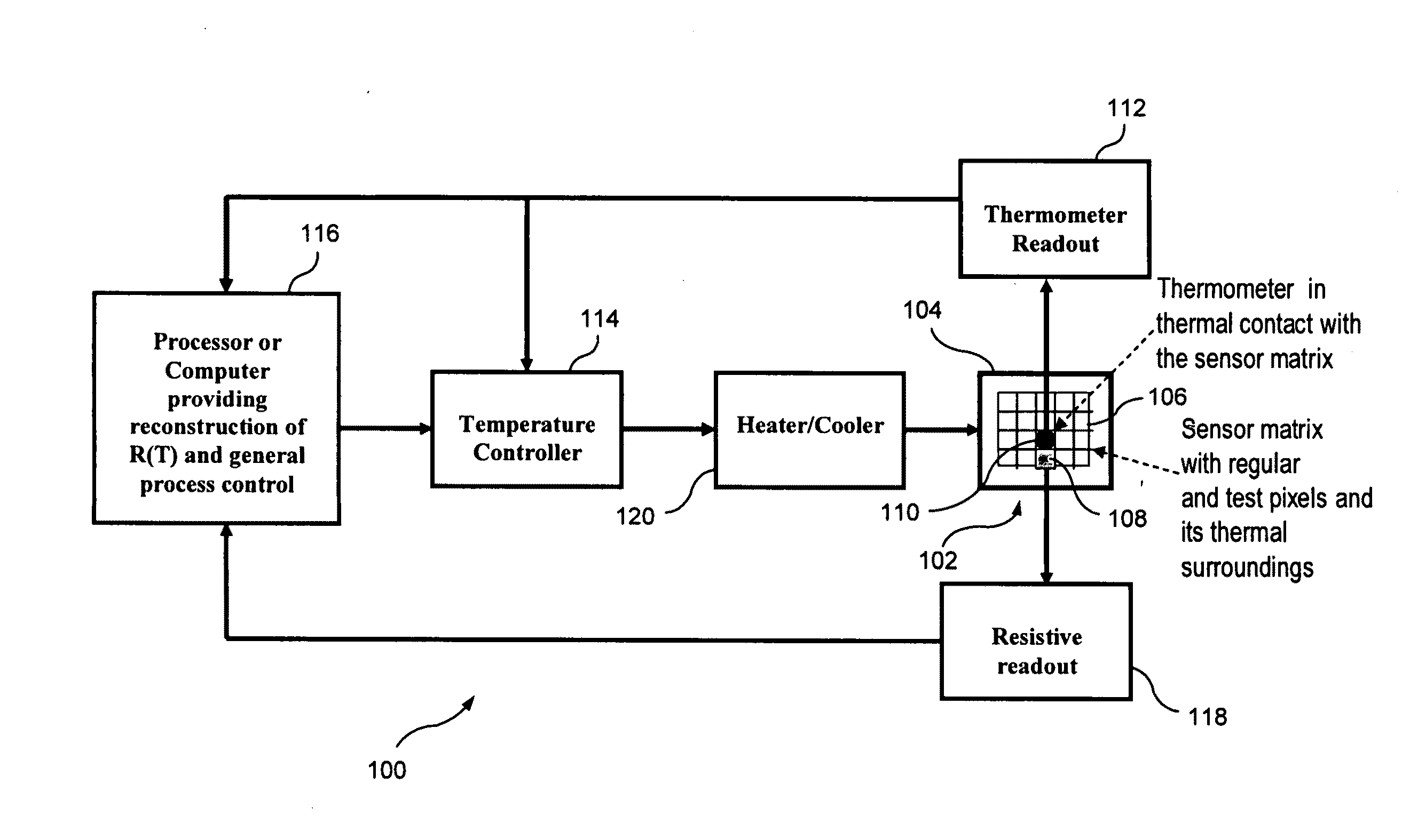
Bolometric sensor with high TCR and tunable low resistivity
- Summary
- Abstract
- Description
- Claims
- Application Information
AI Technical Summary
Benefits of technology
Problems solved by technology
Method used
Image

Examples
Embodiment Construction
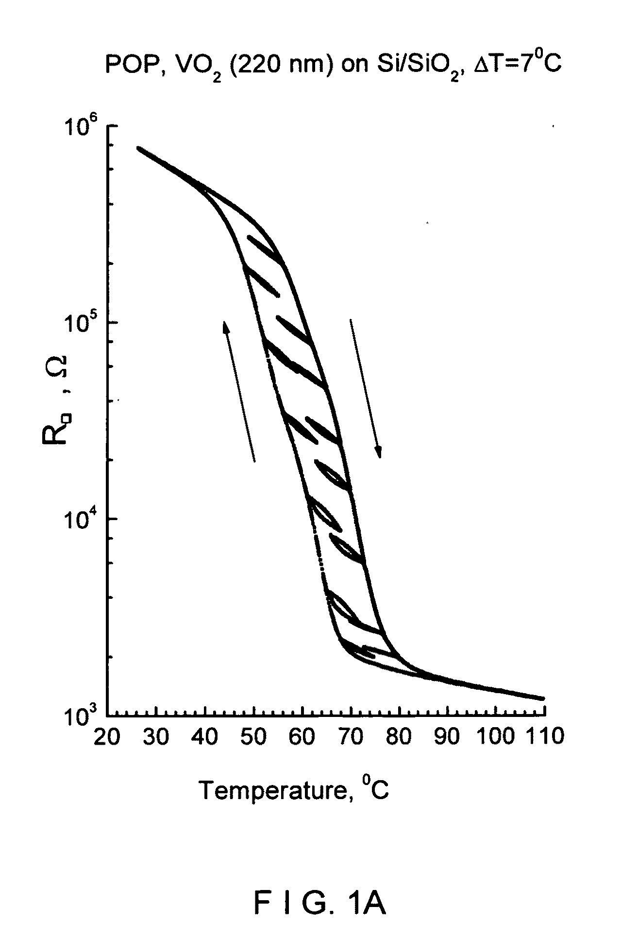
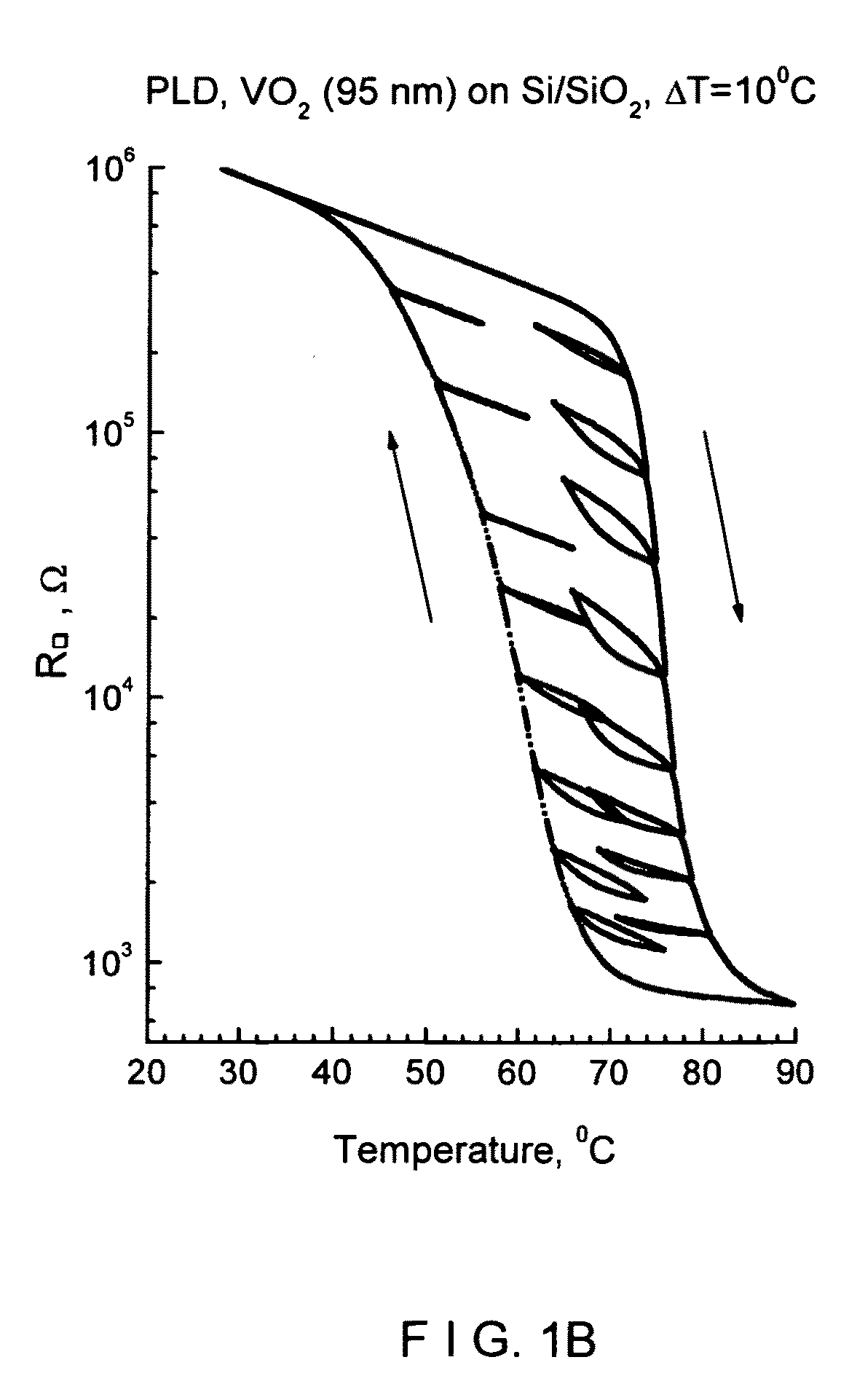
[0047]It is known from prior art that minor hysteresis loops can be generated inside the major hysteresis loop in the resistivity of VO2 films. These minor loops can be initiated at any attachment temperature T0 on the major loop by making what is referred as a “backward round-trip excursion” from that temperature. For T0 on a heating branch this excursion consists of cooling down and then warming up back to T0, and for T0 on a cooling branch it takes place in reverse order: first warming up and then cooling down. Using mathematical symbols, for T0 on the heating branch (FIB), the backward roundtrip excursion denotes a T0→T0−ΔT→T0 process, i.e. cooling down from T0 to T0−ΔT and then warming up by ΔT back to T0. In this invention, it is assumed that ΔT>0 and will be referred to a positive quantity; ΔT as the excursion length, or simply as an excursion. On the cooling branch (CB) the backward direction is that of warming up, and so the backward roundtrip excursion is T0→T0+ΔT→T0. Excu...
PUM
 Abstract
Description
Claims
Application Information