Scan signal transmission system and method thereof

a signal transmission system and signal transmission technology, applied in the field of scanning signal transmission system, can solve the problems of inability to solve the flickering problem, and the inability of chamferic to work well to eliminate the flickering phenomenon any more, so as to reduce the design and production costs of the display device, and the effect of constant visual

Inactive Publication Date: 2011-10-20
CHUNGHWA PICTURE TUBES LTD
View PDF4 Cites 7 Cited by
  • Summary
  • Abstract
  • Description
  • Claims
  • Application Information

AI Technical Summary

Benefits of technology

[0014]The present invention is characterized in that, in the scan operation of two continuous frames, the transmission directions of the scan signal in the pixel scan lines are reversed, and thus the electric coupling effects of each pixel circuit in two frame scan operations are presented in opposite modes, such that the brightness and colorfulness of the display frame of the display device achieve a constant visual effect, thereby reducing the flickering effect generated by the display device, which can be applied to display devices of various sizes. Moreover, it is unnecessary for the manufactures to dispose the chamfered IC on the display device, thus reducing the design and production costs of the display device.

Problems solved by technology

However, the above solution of eliminating the flickering phenomenon cannot solve the flickering problem in an LCD device having a large area.
In the LCD device having a large area, the number of pixel circuits dramatically increases as the display area is enlarged, and the scan signal Vg may be totally deformed as the number of passed pixel circuits increases, such that the chamfered IC cannot work well to eliminate the flickering phenomenon any more.
Therefore, how to provide a solution suitable for LCD devices of any size and eliminating the flickering phenomenon of the LCD devices has become a problem for being solved by the manufacturers.

Method used


Image

  • Scan signal transmission system and method thereof
  • Scan signal transmission system and method thereof
  • Scan signal transmission system and method thereof

Examples


Embodiment Construction

[0024]Preferred embodiments of the present invention are illustrated in detail below with reference to the accompanying drawings.

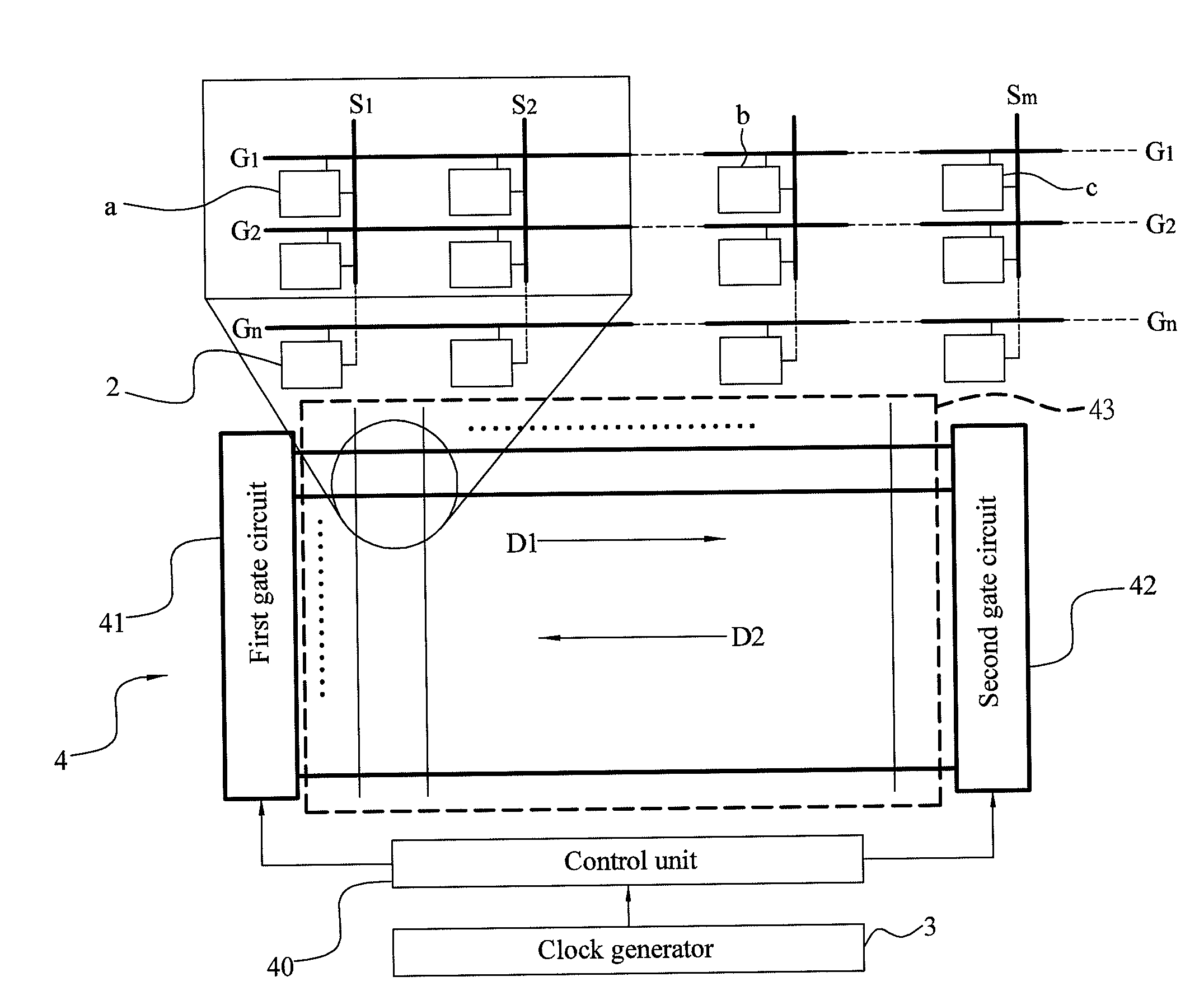
[0025]FIG. 2 is a schematic view of system architecture of a scan signal transmission system according to an embodiment of the present invention. Referring to FIG. 2, the system provided in this embodiment is applicable to a display device (not shown), and the display device includes a display area circuit 43. The display area circuit 43 includes a plurality of pixel circuits 2, a plurality of pixel scan lines (G1˜Gn) is connected to the pixel circuits 2, each of the pixel scan lines (G1˜Gn) is individually connected to the pixel circuits 2 in one row, each of the pixel scan lines (G1˜Gn) is connected to a gate circuit 4, and the gate circuit 4 is further electrically connected to a clock generator 3.

[0026]The clock generator 3 is used for periodically generating at least one scan signal, and transmitting the scan signal to the gate circuit 4. The gate cir...


PUM


Abstract

A scan signal transmission system and a method thereof are provided, which are applicable to a display device. The system includes a display area circuit and a gate circuit, the display area circuit has a plurality of pixel scan lines, and the gate circuit is connected to each of the pixel scan lines. The gate circuit is used for obtaining a scan signal from a clock generator, so as to transmit the scan signal to each of the pixel scan lines sequentially. During each frame scan operation, the gate circuit transmits the scan signal to the pixel scan lines in a reverse signal transmission direction.

Description

CROSS-REFERENCE TO RELATED APPLICATION[0001]This application claims the benefit of Taiwan Patent Application No. 099112347, filed on Apr. 20, 2010, which is hereby incorporated by reference for all purposes as if fully set forth herein.BACKGROUND OF THE INVENTION[0002]1. Field of Invention[0003]The present invention relates to a scan signal transmission system of a liquid crystal display (LCD) device, and more particularly to a scan signal transmission system and a method thereof, which are applicable to transmit a scan signal to each pixel scan line in reverse signal transmission directions during two continuous frame scan operations.[0004]2. Related Art[0005]Referring to FIGS. 1A, 1B, 1C, and 1D together, FIG. 1A is a schematic view of a configuration and a parasitic capacitance of a pixel circuit in the prior art, FIG. 1B is a schematic view of an ideal voltage of the pixel circuit in the prior art, FIG. 1C is a schematic view of a practical voltage of the pixel circuit in the pr...

Claims


Application Information

Patent Timeline
Patent Type & Authority Applications(United States)
IPC IPC(8): G09G5/00
CPCG09G3/3648G09G3/3688G09G3/3614G09G2320/0219
Inventor CHANG, CHIA-HSIENLIN, SHU-YANG
Owner CHUNGHWA PICTURE TUBES LTD
Why Eureka
Try Eureka