Thin film transistor, array substrate and liquid crystal display panel

Active Publication Date: 2017-05-11
TCL CHINA STAR OPTOELECTRONICS TECH CO LTD
View PDF5 Cites 2 Cited by
  • Summary
  • Abstract
  • Description
  • Claims
  • Application Information

AI Technical Summary

Benefits of technology

The present invention provides a thin film transistor, array substrate and liquid crystal display panel that keeps the field effect mobility of a nitrogen-doped AOS TFT device constant. This is achieved by using a nitrogen-doped oxide semiconductor layer and a non-nitrogen doped oxide semiconductor layer wherein enough oxygen vacancies are maintained in the active layer. This results in a more reliable thin film transistor and reduced manufacturing costs.

Problems solved by technology

However, doping nitrogen generally causes a decline in mobility, which is unfavorable to the manufacturing of AOS TFT devices having high mobility for meeting the engineering application requirements in the field of panel displays.

Method used


Image

  • Thin film transistor, array substrate and liquid crystal display panel
  • Thin film transistor, array substrate and liquid crystal display panel
  • Thin film transistor, array substrate and liquid crystal display panel

Examples


first embodiment

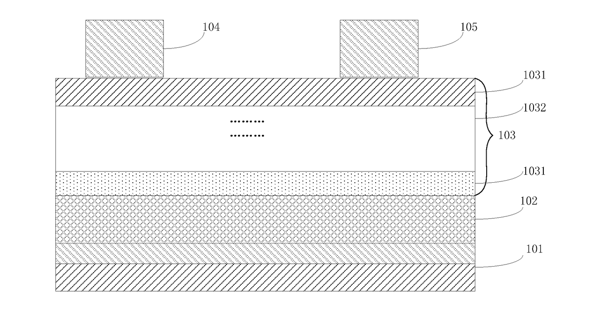
[0058]As shown in FIG. 1, the present embodiment provides a thin film transistor (for example, AOS TFT), including: a gate electrode 101, a gate insulating layer 102, an active layer 103, and a source electrode 104 and a drain electrode 105 of the thin film transistor.

[0059]In the present embodiment, the gate insulating layer 102 is located on the gate electrode 101, and can be formed by chemical deposition; the active layer 103 is located on the gate insulating layer 102, and can be formed by chemical deposition, wherein the material forming the active layer 103 can be a nitrogen-doped amorphous oxide semiconductor, such as nitrogen-doped a-IGZO and the like.

[0060]In the present embodiment, the active layer 103 is formed from the nitrogen-doped oxide semiconductor layer 1031 and the non-nitrogen doped oxide semiconductor layer 1032. In FIG. 1, the active layer 103 includes at least two of the nitrogen-doped oxide semiconductor layers 1031 and at least one of the non-nitrogen doped ...

second embodiment

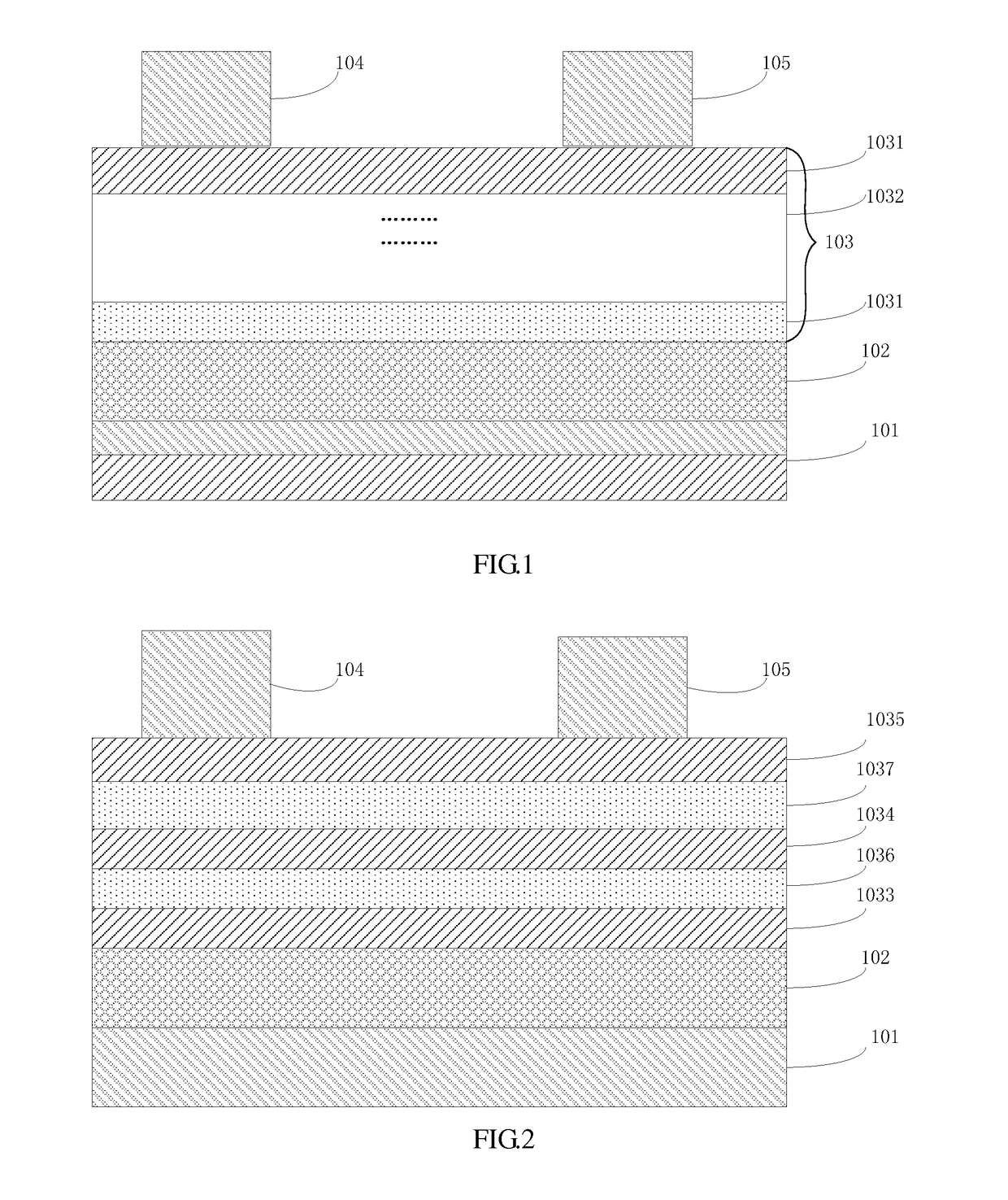
[0073]An array substrate of a liquid crystal display panel is provided in the present embodiment, as shown in FIG. 4, including a substrate 401 on which a plurality of data lines (not shown in the FIGs.), a plurality of scan lines (not shown in FIGs.), a plurality of pixel electrodes 402, and a thin film transistor 403 are located. The thin film transistor 403 specifically includes a gate electrode 4031 which is formed on the substrate 401, a gate insulating layer 4032 which is formed on the gate electrode 4031, an active layer 4033 which is formed on the gate insulating layer 4032, and a source electrode 4034 and a drain electrode 4035 which are respectively formed on both sides of the active layer 4033.

[0074]The data lines are used for transmitting data signals to a corresponding source electrode of the thin film transistor. The scan lines are used for transmitting scan signals to a corresponding gate electrode of the thin film transistor. The thin film transistor 403 is used for ...

third embodiment

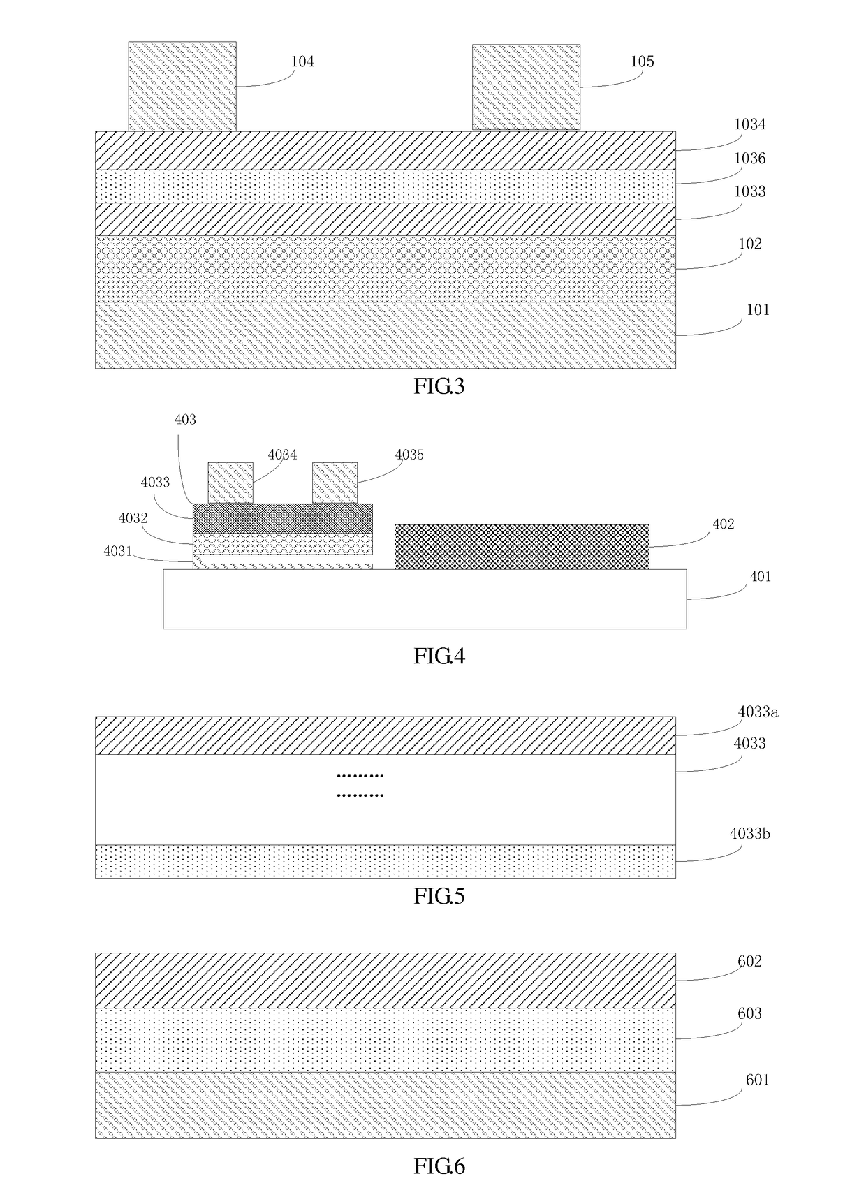
[0088]A liquid crystal display panel is provided in the present embodiment, as shown in FIG. 6, including a color filter substrate 601, an array substrate 602, and a liquid crystal layer 603 disposed between the color filter substrate 601 and the array substrate 602. The structure of the array substrate 602, as referred to FIG. 4, includes a substrate, on which a plurality of data lines, a plurality of scan lines, a plurality of pixel electrodes, and a thin film transistor 403 are located. The data lines are used for transmitting data signals to a corresponding source electrode of the thin film transistor. The scan lines are used for transmitting scan signals to a corresponding gate electrode of the thin film transistor. The thin film transistor is used for controlling whether to transfer the data signals to the corresponding pixel electrodes through the drain electrode of the thin film transistor based on the scan signals. The thin film transistor specifically includes a gate elect...


PUM


Abstract

A thin film transistor, an array substrate and a liquid crystal display panel are provided. The thin film transistor has an active layer which is formed from nitrogen-doped oxide semiconductor layers and a non-nitrogen doped oxide semiconductor layer. By disposing the non-nitrogen doped oxide semiconductor layer in the active layer of the nitrogen-doped thin film transistor, the mobility of the thin film transistor is kept constant for improving the reliability of the thin film transistor.

Description

FIELD OF THE INVENTION[0001]The present invention relates to the technical field of liquid crystal displays, and particularly to a thin film transistor, an array substrate and a liquid crystal display panel.BACKGROUND OF THE INVENTION[0002]Amorphous oxide semiconductor (AOS) thin film transistors (TFT) have favorable electrical properties, high transparency and low temperature in the manufacturing process, etc., so as to attract considerable people's attention, and are one of the most powerful competitors of active electronic devices for driving displays of a new generation of panels. Common AOS TFTs include an indium gallium zinc oxide thin film transistor (IGZO TFT), a IZO TFT, a ZTO TFT, etc.[0003]In order to improve certain electrical indexes and stability of TFT devices, the level of oxygen vacancies in the active layer of the AOS TFT is conventionally regulated by nitrogen, that is, nitrogen is doped in the active layer of the AOS TFT. This type of AOS TFT is referred to as a ...

Claims


Application Information

Patent Timeline
IPC IPC(8): H01L29/786G02F1/1335G02F1/1368G02F1/1362H01L29/49H01L27/12
CPCH01L29/78696H01L29/78693H01L29/4908H01L27/1225H01L27/124G02F2202/10G02F1/1368G02F1/136286G02F1/133514H01L2029/42388G02F2201/123H01L27/127H01L27/1214H01L29/78681H01L29/7869H01L29/42384
Inventor LI, SHAN
Owner TCL CHINA STAR OPTOELECTRONICS TECH CO LTD
Why Eureka
Try Eureka