Optical processing apparatus and optical processing method

Inactive Publication Date: 2006-07-18
SEMICON ENERGY LAB CO LTD
View PDF33 Cites 2 Cited by
  • Summary
  • Abstract
  • Description
  • Claims
  • Application Information

AI Technical Summary

Benefits of technology

[0022](2) To provide a technique capable of performing laser light illumination while making control for always maintaining the optimum condition in a process of improving the quality of a thin film and annealing of a thin film both using laser light.
[0023](3) To provide a technique capable of easily evaluating the crystallinity of a silicon thin film in a crystallization process of a silicon thin film using laser light.
[0024](4) To provide a technique capable of easily evaluating the crystallinity of a silicon thin film and the flatness of its surface in a crystallization process of a silicon thin film using laser light.
[0043]The above method is characterized in that the silicon film to be irradiated with laser light is a film that has been crystallized with the aid of at least one element for facilitating crystallization. The at least one element may be one or a plurality of elements selected from Ni, Pd, Pt, Cu, Ag, Au, In, Sn, Pb, As and Sb. In particular, remarkable effects can be obtained when Ni is used. Specifically, an amorphous silicon film can be crystallized to obtain a crystalline silicon film by introducing the element for facilitating crystallization into the amorphous silicon film and the subjecting it to a heat treatment. The heat treatment can be performed at a temperature lower more than 50° C. compared with the case where no catalyst element for facilitating crystallization is used. In addition, heating damage to the substrate (particularly a glass substrate) can be greatly reduced.
[0051]For example, FIG. 4 shows experimental data representing a relationship between the irradiation energy density of laser light and the refractive index n of a silicon thin film whose crystallinity has been improved by the laser light irradiation. Based on this graph, the refractive index of a silicon thin film can be made close to a predetermined value by increasing the laser light irradiation energy density in the next irradiating operation when the refractive index n of a silicon thin film is larger than a predetermined value, and decreasing the laser light irradiation energy density in the next irradiating operation when the refractive index n of a silicon thin film is smaller than the predetermined value.

Problems solved by technology

However, the excimer laser light is associated with a problem that its illumination energy is unstable, resulting in a difficulty in keeping the optimum illuminating condition.
Therefore, there exists a problem originating from the principle that when laser oscillation is continued, increase of impurities in the gas or change in quality of the gas itself lowers the laser light output even with application of the same discharge power.
But this is not always satisfactory.
(1) Bad reproducibility of measurements.
(2) Use of a large-output laser such as an Ar laser causes a problem in safety.
(3) An expensive apparatus is needed.
(4) A measurement takes long time.
Thus, a crystalline silicon film to be used for a thin-film transistor having desired characteristics cannot be evaluated sufficiently only by the Raman spectroscopy.
However, as described above, the illumination energy of excimer laser light is liable to vary and it is difficult to control the illumination energy.

Method used


Image

  • Optical processing apparatus and optical processing method
  • Optical processing apparatus and optical processing method
  • Optical processing apparatus and optical processing method

Examples


embodiment 1

[0060]This embodiment is directed to a system and a method of evaluating states (which are defined as a concept including the crystallinity and the flatness of a film) of a silicon film that has been crystallized by illumination with excimer laser light.

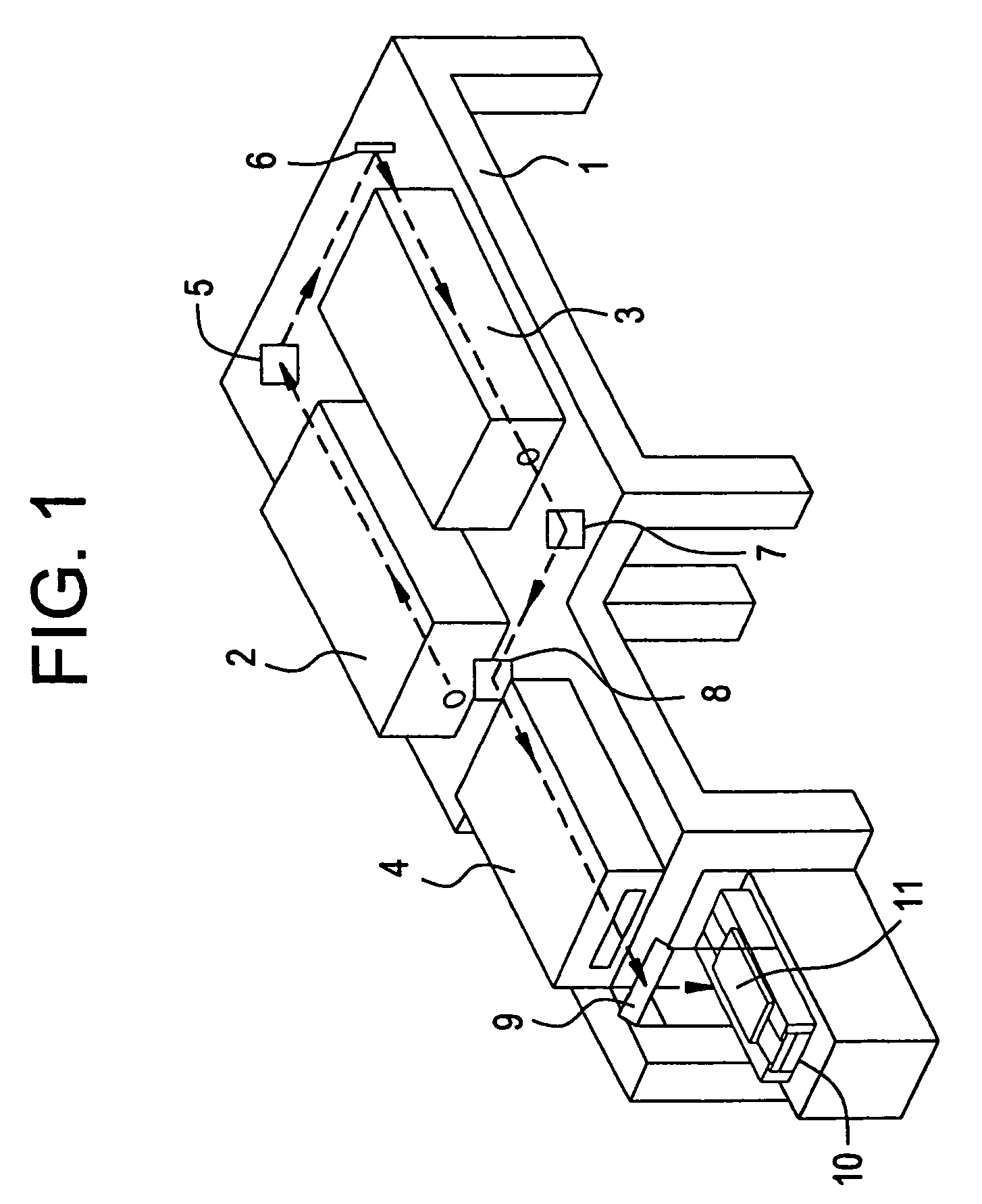
[0061]First, a description will be made of an apparatus. FIG. 1 is a conceptual diagram of a laser annealing apparatus used in this embodiment. KrF excimer laser light (wavelength: 248 nm; pulse width: 25 ns) is emitted from an oscillator 2. Apparently other excimer lasers and lasers of other types can also be used.

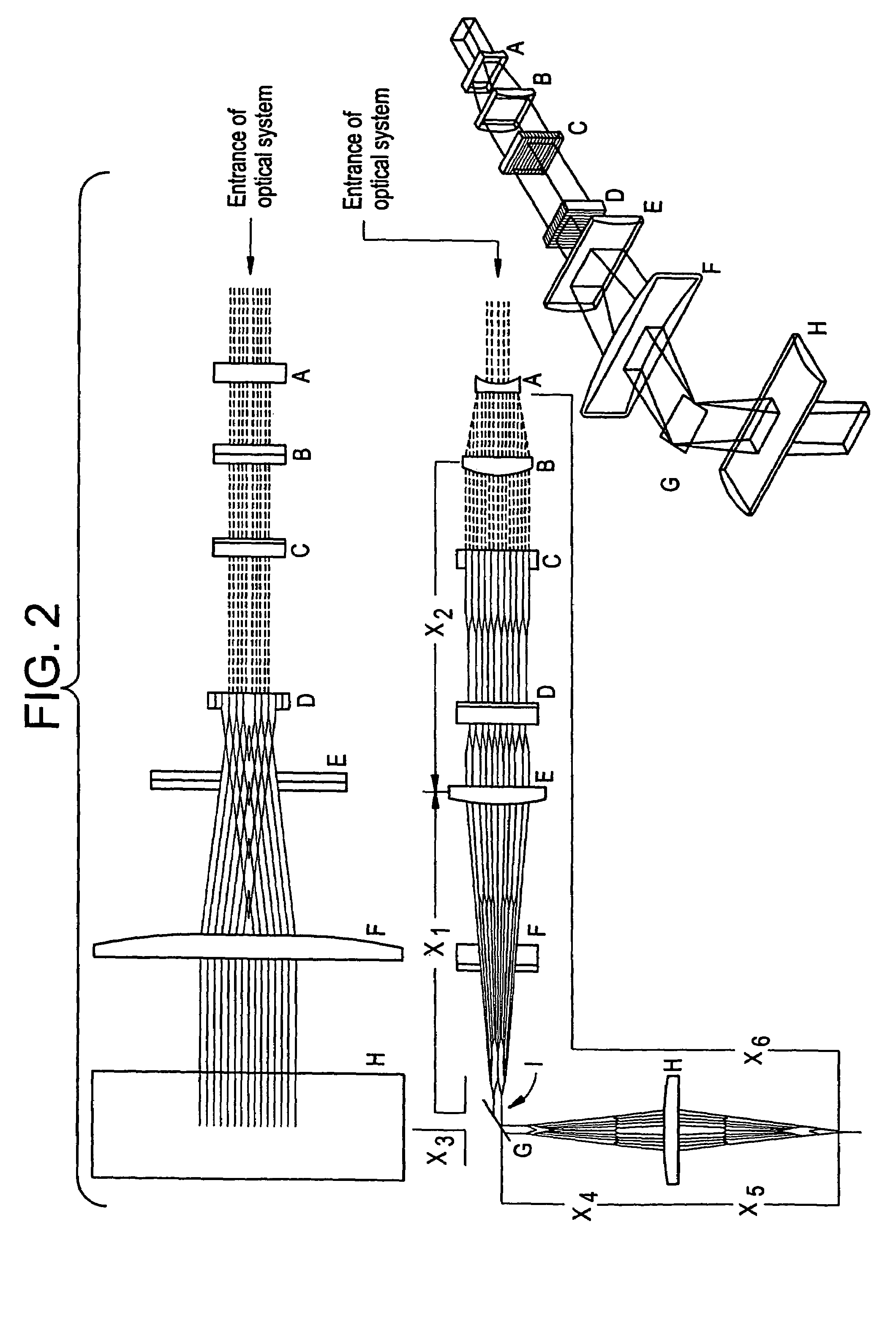
[0062]Laser light emitted from the oscillator 2 are passed through full-reflection mirrors 5 and 6, amplified by an amplifier 3, and introduced into an optics 4 via full-reflection mirrors 7 and 8. The laser beam, which has a rectangular shape of about 3×2 cm2 before entering the optics 4, is shaped by the optics 4 into a long and narrow beam (linear beam) of 10–30 cm in length and 0.1–1 cm in width. The laser light as out...

embodiment 2

[0083]This embodiment is directed to formation of a thin-film transistor by use of the technique of the first embodiment. FIGS. 5(A)–5(D) show manufacturing steps of a thin-film transistor. In this embodiment, a glass substrate 501 is used as the substrate. A 2,000-Å-thick silicon dioxide film (not shown) is formed, as an undercoat film, on the surface of the glass substrate 501.

[0084]First, a 500-Å-thick amorphous silicon film 502 is formed on the glass substrate 501 by plasma CVD or low-pressure thermal CVD. Ultraviolet light is then applied to the surface of the amorphous silicon film 502 in an oxygen atmosphere. After the surface is cleaned, a very thin oxide film is formed on the cleaned surface. A solution of nickel acetate is applied to form a liquid film 503, and then spin-coated with a spinner 500 (see FIG. 5(A)).

[0085]Next, the substrate is subjected to a heat treatment of 450° C. for one hour in an inert gas atmosphere to remove hydrogen from the amorphous silicon film 50...

embodiment 3

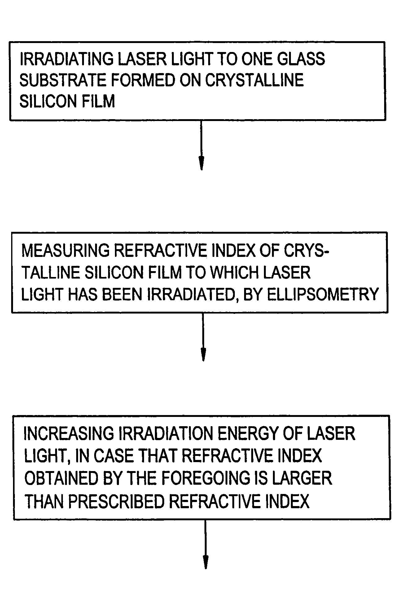
[0096]This embodiment is directed to a technique of correcting the laser light illumination conditions on a realtime basis. The data of FIG. 4 represent a relationship between refractive indices (as measured by the ellipsometry) of crystalline silicon films whose crystallinity has been improved by illumination with KrF excimer laser light and illumination energy densities (mJ / cm2) of laser light used. As mentioned above, the illumination energy densities of FIG. 4 do not represent actual energy densities of laser light used.

[0097]However, it is understood that the refractive index of a crystallinity-improved crystalline silicon film and the energy density of illumination laser light has a relative relationship that is proportional as shown in FIG. 4. Therefore, by constantly controlling the laser light illumination energy so as to provide a predetermined refractive index, a constant illumination energy density value can always be obtained.

[0098]Therefore, where it is necessary to pe...


PUM


Abstract

In an annealing process in which laser light is irradiated to a semiconductor thin film, a refractive index of the semiconductor thin film after laser light irradiation is measured and conditions for the next laser light irradiation are adjusted based on the measured refractive index value. For example, laser light irradiation conditions are adjusted so that semiconductor thin films always have the same refractive index. As a result, the annealing can be performed under the same conditions at every laser light irradiation even if the laser light irradiation conditions vary unavoidably.

Description

[0001]This application is a Division of Ser. No. 10 / 035,441 Jan. 4, 2002 U.S. Pat. No. 6,716,283 which is a Division of Ser. No. 09 / 547,716 Apr. 11, 2000 U.S. Pat. No. 6,336,969 which is a Division of Ser No. 08 / 451,648 May 26, 1995 U.S. Pat. No. 6,059,873.BACKGROUND OF THE INVENTION[0002]The present invention relates to a technique of evaluating a processing effect of various processes using laser light. The invention also relates to a technique of relatively evaluating and controlling illumination energy of laser light.[0003]“Low-temperature processes” are now being developed to manufacture a liquid crystal panel using polysilicon thin-film transistors (TFTs). This is intended to suppress the cost of a liquid crystal panel itself by using a low-temperature process, which allows use of a glass substrate with which a large-size substrate can be obtained at a low cost.[0004]To realize a low-temperature process, the key subject is to crystallize an amorphous silicon film formed on a g...

Claims


Application Information

Patent Timeline
IPC IPC(8): H01L21/00C30B13/24
CPCC30B13/24Y10S117/904
Inventor YAMAGUCHI, NAOAKITANAKA, KOICHIROTERAMOTO, SATOSHI
Owner SEMICON ENERGY LAB CO LTD
Why Eureka
Try Eureka