

Uninterrupted power supply apparatus
- Summary
- Abstract
- Description
- Claims
- Application Information
AI Technical Summary
Benefits of technology
Problems solved by technology
Method used
Image

Examples
first embodiment
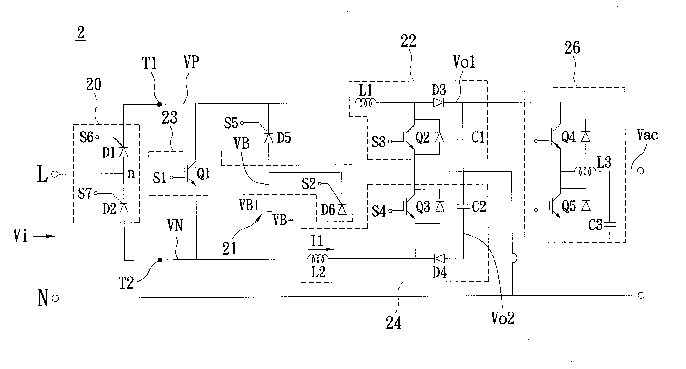
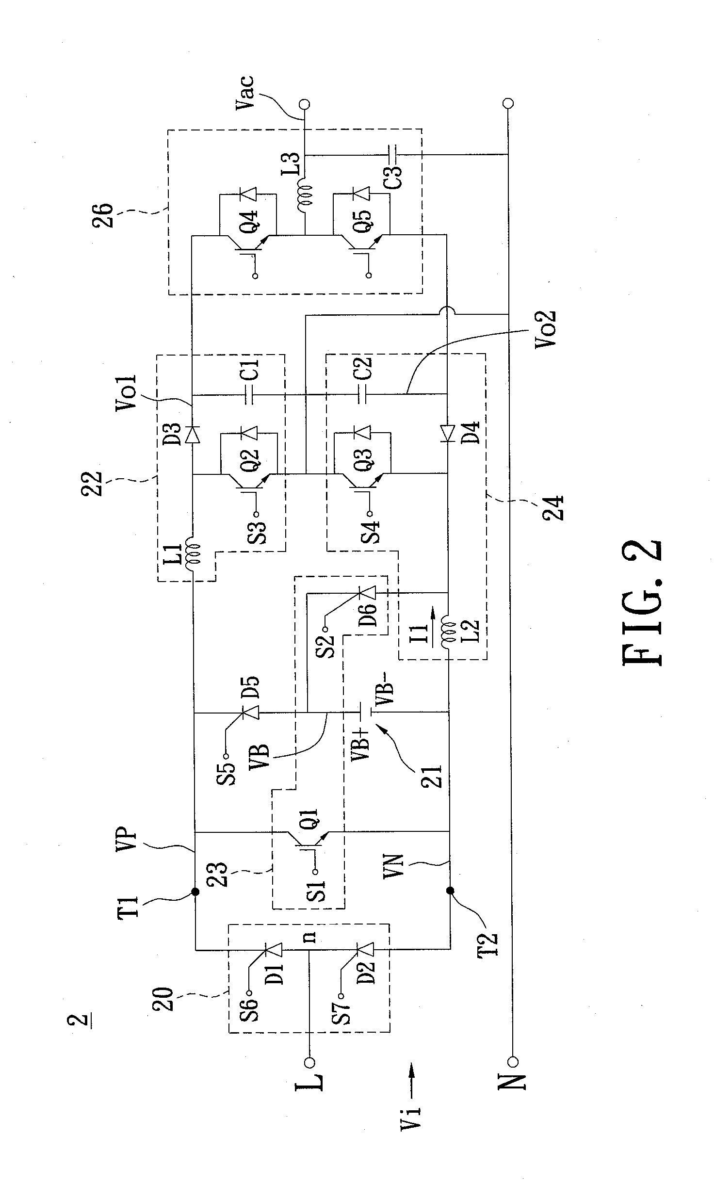
[0017]Please refer to FIG. 2, in which a circuit schematic diagram of an uninterrupted power supply apparatus in accordance with certain aspects of the present invention is demonstrated. An uninterrupted power supply apparatus 2 comprises a rectifying unit 20, a backup battery 21, a first boost unit 22, a charge circuit 23, a second boost unit 24, and current shunt unit 26. herein, the rectifying unit 20 is composed of two silicon controlled rectifier D1, D2, which has a node n, a positive output terminal T1, and a negative output terminal T2, in which the node n couples to an AC power line L.
[0018]The rectifying unit 20 rectifies an AC input power Vi successively and outputs a positive half-cycle of voltage potential VP and a negative half-cycle of voltage potential from the positive output terminal T1 and the negative output terminal T2 respectively and alternatively. Meanwhile, the backup battery 21 has a positive terminal VB+ and a negative terminal VB−, for outputting a backup ...
third embodiment
[0031]Please refer to FIG. 4, in which a circuit schematic diagram of an uninterrupted power supply apparatus in accordance with certain aspects of the present invention is demonstrated. An uninterrupted power supply apparatus 3 according to the present invention is provided. The uninterrupted power supply apparatus 3 comprises a rectifying unit 20, a backup battery 21, a first boost unit 32, a charge circuit 22, a second boost unit 34, and a current shunt unit 36. Herein, the rectifying unit 33 is composed of two silicon controlled rectifiers D1, D2, which have a node n inbetween, a positive output terminal T1 and a negative output terminal T2 and the node N couples to an AC power line L.
[0032]The rectifying unit 30 rectifies an AC input power Vi successively and outputs a positive half-cycle of voltage potential VP and a negative half-cycle of voltage potential from the positive output terminal T1 and the negative output terminal T2 respectively and alternatively. Meanwhile, the b...
PUM
 Abstract
Description
Claims
Application Information