Clock signal duty correction circuit
- Summary
- Abstract
- Description
- Claims
- Application Information
AI Technical Summary
Benefits of technology
Problems solved by technology
Method used
Image

Examples
Embodiment Construction
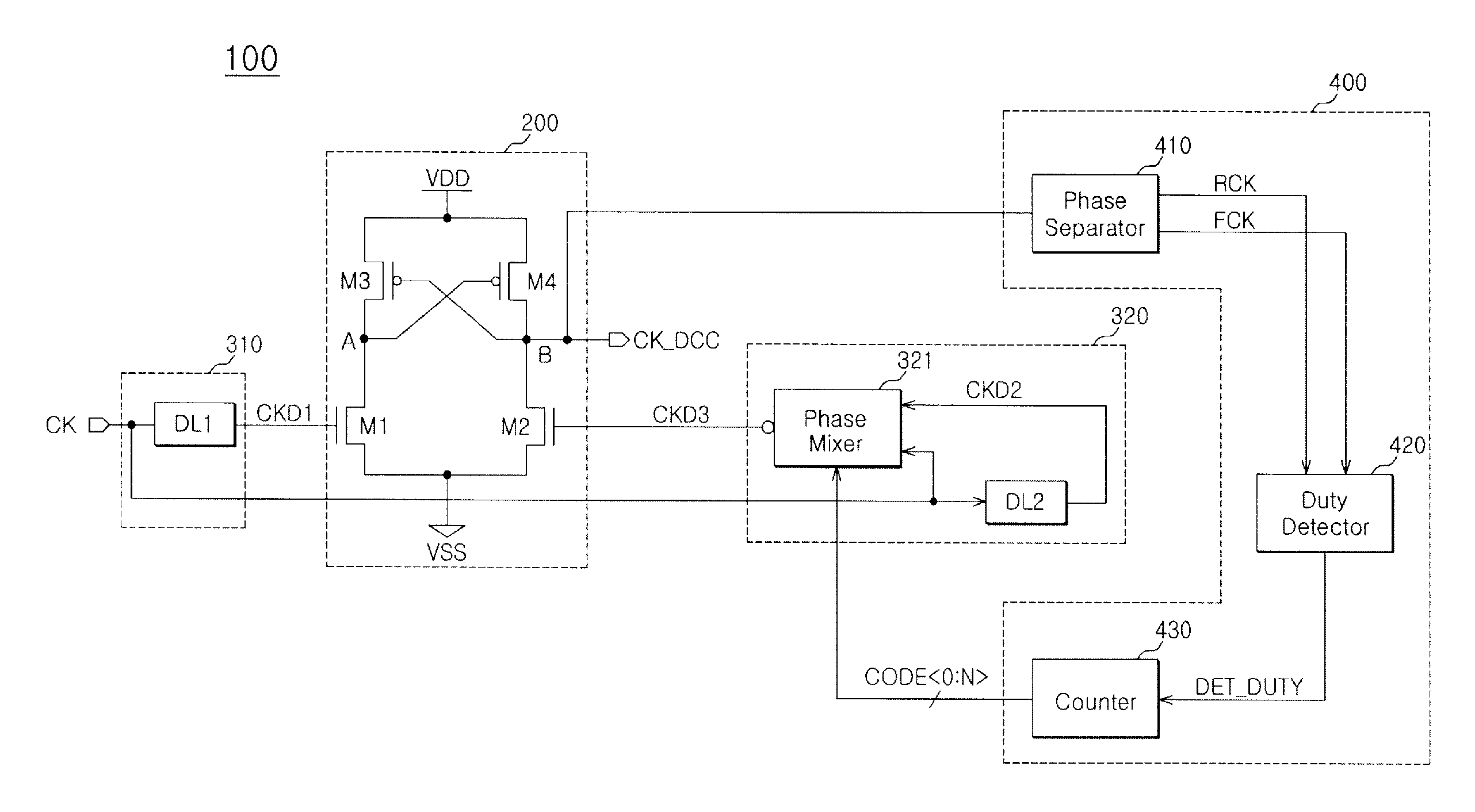
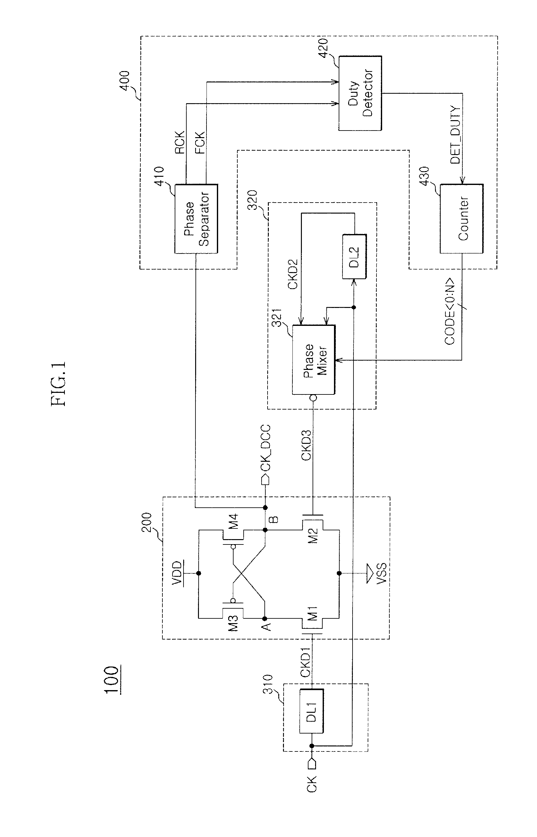
[0014]Hereinafter, a clock signal duty correction circuit according to the present invention will be described below with reference to the accompanying drawings through exemplary embodiments.
[0015]As illustrated in FIG. 1, a clock signal duty correction circuit 100 according to an embodiment of the present invention includes a first transition timing control unit 310, a second transition timing control unit 320, a differential buffer unit 200, and a control code generation unit 400.
[0016]The first transition timing control unit 310 is configured to generate a first control signal, which is a first delay clock signal CKD1, by using a clock signal CK for controling the rising timing of a duty correction clock signal CK_DCC.
[0017]The first transition timing control unit 310 includes a first delay unit DL1.
[0018]The first delay unit DL1 is configured to delay the clock signal CK by a first delay time and generate the first delay clock signal CKD1.
[0019]The second transition timing contr...
PUM
 Abstract
Description
Claims
Application Information
 - R&D
- Intellectual Property
- Life Sciences
- Materials
- Tech Scout
- Unparalleled Data Quality
- Higher Quality Content
- 60% Fewer Hallucinations
Browse by: Latest US Patents, China's latest patents, Technical Efficacy Thesaurus, Application Domain, Technology Topic, Popular Technical Reports.
© 2025 PatSnap. All rights reserved.Legal|Privacy policy|Modern Slavery Act Transparency Statement|Sitemap|About US| Contact US: help@patsnap.com