Lead frame for chip package, chip package, package module, and illumination apparatus including chip package module

a technology for chip packages and package modules, applied in the direction of solid-state devices, light and heating devices, basic electric elements, etc., can solve the problems of increasing manufacturing costs, and achieve the effect of simplifying the packaging process and facilitating the arrangement of the circuit of the chip packages

Active Publication Date: 2011-11-10
SAMSUNG ELECTRONICS CO LTD
View PDF1 Cites 23 Cited by
  • Summary
  • Abstract
  • Description
  • Claims
  • Application Information

AI Technical Summary

Benefits of technology

[0007]Provided are lead frames for chip packages, chip packages, package modules, and illumination apparatuses, in which structures of chip packages are improved to simplify a packaging process and to easily arrange a circuit of the chip packages.

Problems solved by technology

Thus, since a multistep packaging process is required to use chips in electronic devices, manufacturing costs may be increased.

Method used


Image

  • Lead frame for chip package, chip package, package module, and illumination apparatus including chip package module
  • Lead frame for chip package, chip package, package module, and illumination apparatus including chip package module
  • Lead frame for chip package, chip package, package module, and illumination apparatus including chip package module

Examples


Embodiment Construction

[0097]Reference will now be made in detail to embodiments, examples of which are illustrated in the accompanying drawings, wherein like reference numerals refer to the like elements throughout, and the thicknesses of layers and regions are exaggerated for clarity.

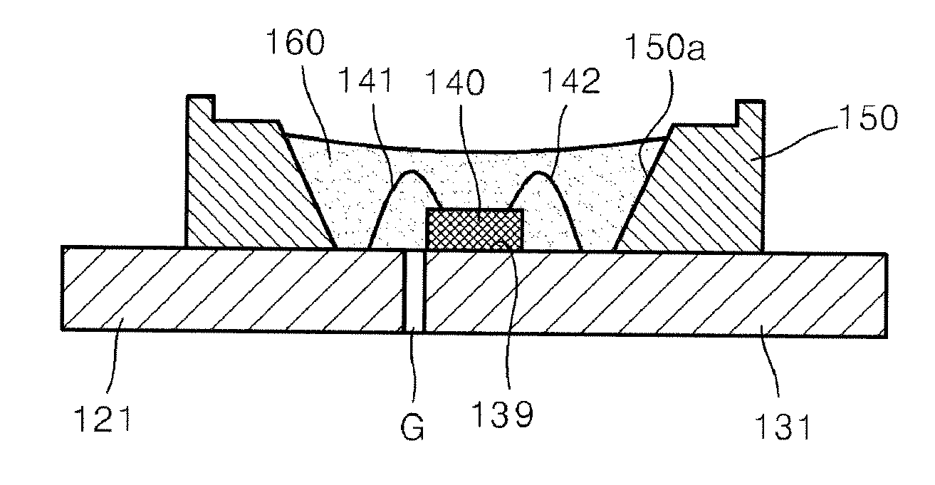
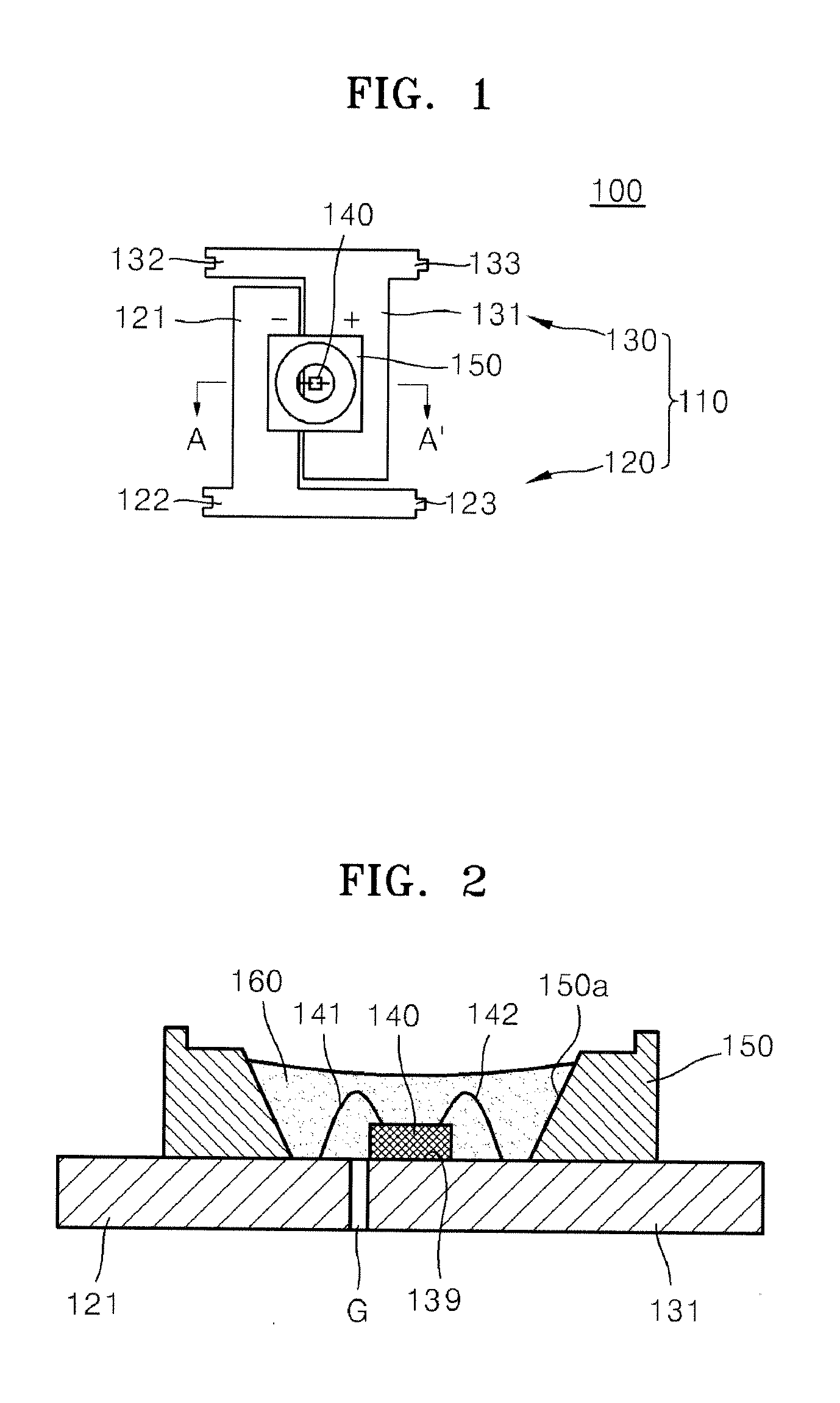
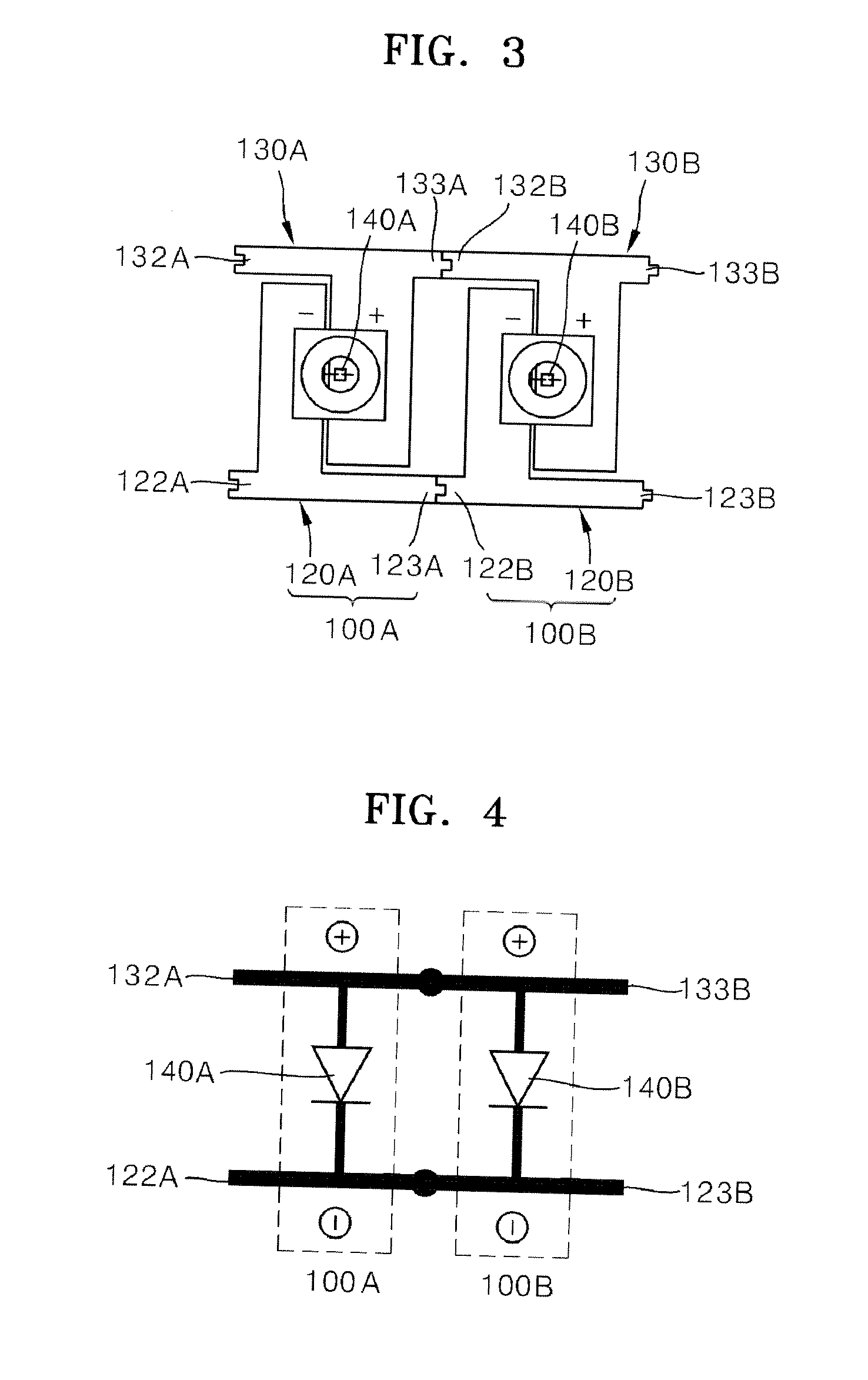
[0098]FIG. 1 is a schematic plan view of a chip package 100 according to an embodiment of the present invention. FIG. 2 is a cross-sectional view of the chip package 100 of FIG. 1 taken along a line A-A′.

[0099]Referring to FIGS. 1 and 2, the chip package 100 includes a light-emitting device chip 140, a lead frame 110 for electrically connecting the light-emitting device chip 140 to an external device, and a reflective cavity 150 for reflecting light emitted from the light-emitting device chip 140 to guide the light outwards.

[0100]The lead frame 110 may be formed of a conductive metal such as aluminum (Al), or copper (Cu) by using a press process, an etching process, or the like. The lead frame 110 includes a first frame por...


PUM


Abstract

A lead frame for a chip package, a chip package, a package module, and an illumination apparatus including the chip package module. The chip package includes a first coupling portion and a second coupling portion that are coupled to each other on edges of a lead frame for mounting a chip thereon, and thus a package module is easily embodied by coupling the first coupling portion and the second coupling portion to each other.

Description

CROSS-REFERENCE TO RELATED APPLICATIONS [0001]This application claims the benefit of Korean Patent Application No. 10-2010-0043171, filed on May 7, 2010, in the Korean Intellectual Property Office, the disclosure of which is incorporated herein in its entirety by reference.BACKGROUND [0002]1. Field[0003]The present disclosure relates to lead frames for chip packages, chip packages, package modules, and illumination apparatuses including the package modules, which are used for packaging a plurality of chips.[0004]2. Description of the Related Art[0005]In general, with regard to chips, a primary packaging process is performed on chips in order to protect the chips and to easily electronically arrange the chips, and then a secondary packaging process is performed in order to mount the chips on a circuit board on which a circuit is formed by the chips together with other components. Thus, since a multistep packaging process is required to use chips in electronic devices, manufacturing c...

Claims


Application Information

Patent Timeline
Patent Type & Authority Applications(United States)
IPC IPC(8): H01L33/62H01L23/495
CPCF21K99/00H01L33/486H01L33/62H01L2224/48091H01L2224/48247H01L2924/3025H01L2224/16245H01L2924/00014H01L2924/00H01L2924/12044
Inventor LEE, YOUNG-JINLEE, JEONG-WOOKMOON, KYUNG-MISONG, YOUNG-HEECHOI, III-HEUNG
Owner SAMSUNG ELECTRONICS CO LTD
Why Eureka
Try Eureka