Imaging apparatus, external flash correction method, recording medium, and integrated circuit

a technology of external flash and recording medium, applied in the field of imaging apparatuses, can solve the problems of white band interference, timing of the accumulation period of respective pixels, and cmos image sensors

Active Publication Date: 2011-11-10
PANASONIC CORP
View PDF7 Cites 13 Cited by
  • Summary
  • Abstract
  • Description
  • Claims
  • Application Information

AI Technical Summary

Benefits of technology

[0057]Accordingly, with this imaging apparatus, it is possible to properly suppress white band interference caused by an external flash from occurring in captured images, even during electronic shutter operations.
[0059]According to this technique, it is possible to realize an imaging apparatus, an external flash correction method, a recording medium, and an integrated circuit capable of obtaining an image (video) in which the influence of a flash is properly suppressed even in the case where the image has been captured using an electronic shutter function

Problems solved by technology

For this reason, CMOS image sensors suffer from deficiencies not found in CCD image sensors because skew in the readout times of accumulated charges causes the timings of the accumulation periods for respective pixels to shift.
One such example of such a problem is a phenomenon in which white band interference occurs when a subject illuminated by the flash of a still camera or the like is captured using a video camera that employs a CMOS image sensor.
There is thus a problem with imaging apparatuses with a CMOS image sensor in that white band interference occurs in the captured signal when an external flash of light such as a flash light or the like occurs.
However, with the aforementioned conventional technique, the influence of the external flash is corrected through the generation of a new image by adding together the two images that have been affected by a flash, and thus in the case where an electronic shutter function, which is a function of an imaging apparatus, is employed, there are situations where the influence of an external flash cannot be properly corrected.
For this reason, in the case of FIG. 12, even if processing according to the stated conventional technique is carried out, two screens (frame images) that have been affected by a flash cannot be added together, and thus the influence of flash light cannot be properly corrected.

Method used


Image

  • Imaging apparatus, external flash correction method, recording medium, and integrated circuit
  • Imaging apparatus, external flash correction method, recording medium, and integrated circuit
  • Imaging apparatus, external flash correction method, recording medium, and integrated circuit

Examples


first embodiment

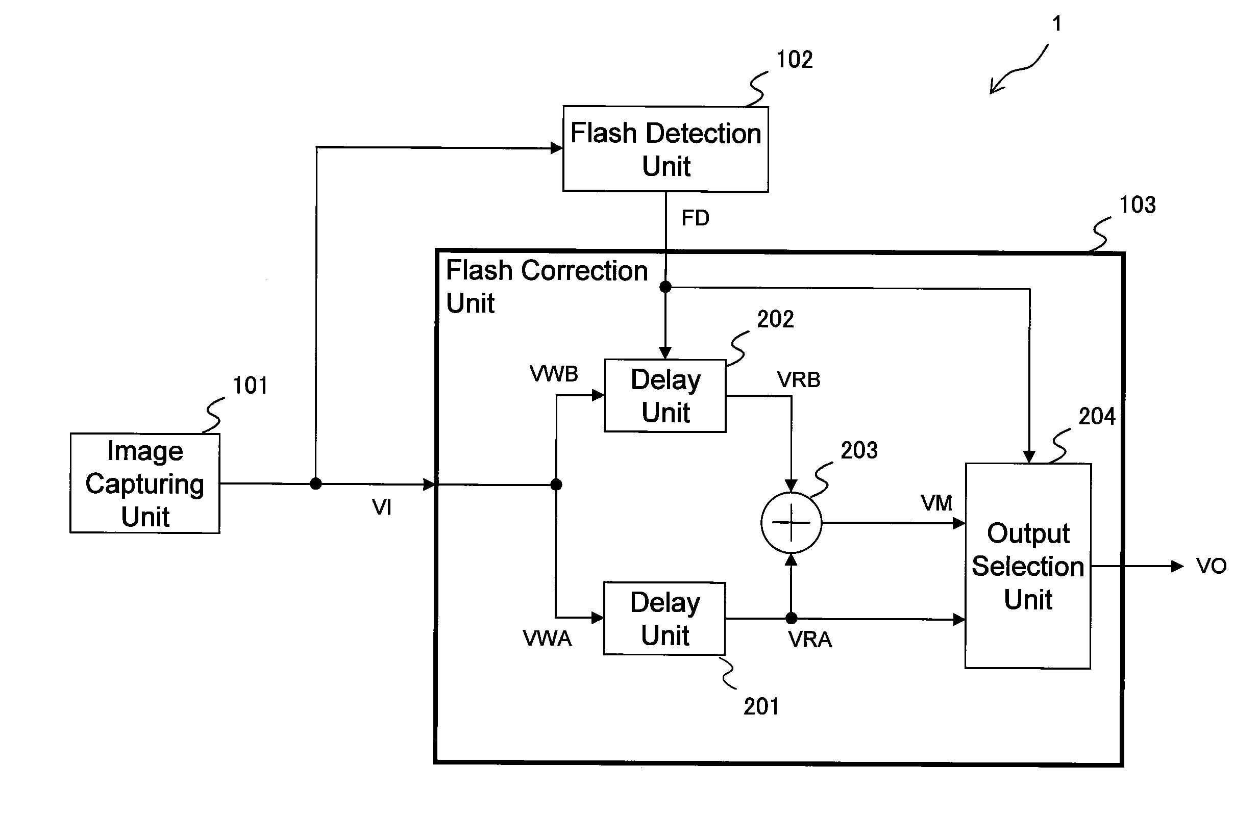
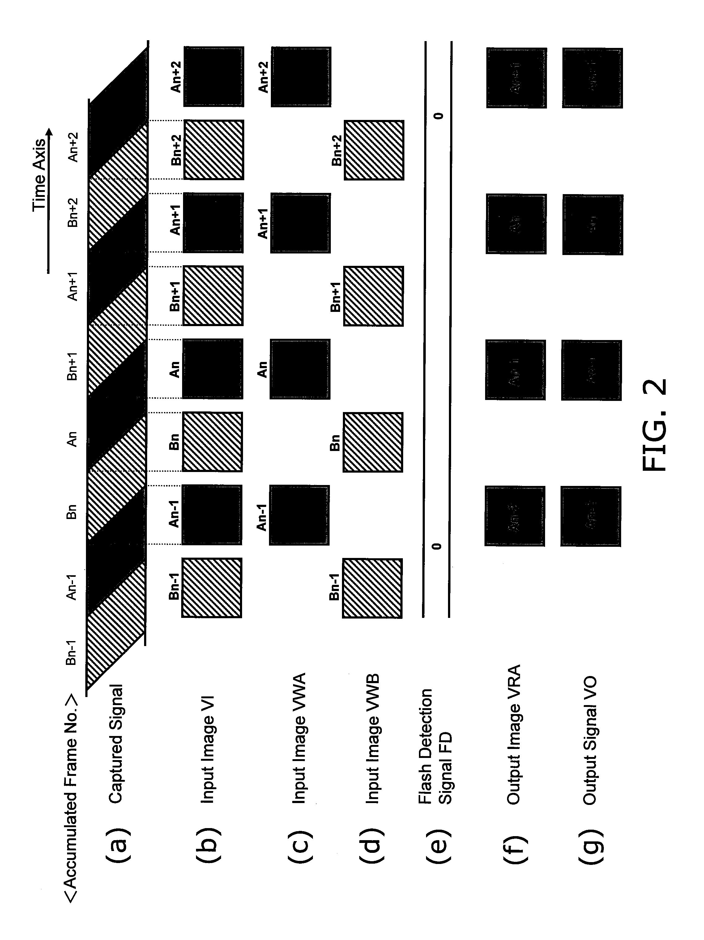
[0075]In the first embodiment, a case in which an imaging apparatus executes processing using an electronic shutter function will be described. Furthermore, in the present embodiment, the descriptions will be given assuming that the exposure time for a single frame (that is, the accumulation time of a signal charge) is approximately equal to ½ of the signal readout cycle determined by the imaging frame rate (that is, a single frame interval). For example, in the case where the imaging frame rate is 24 frames per second and both one frame interval and the signal readout cycle are 1 / 24 second, the exposure time is 1 / 48 second. Finally, the signal charge readout period is assumed to be 1 / 60 second.

[0076]

[0077]FIG. 1 is a diagram illustrating the overall configuration of an imaging apparatus 1 according to the present embodiment.

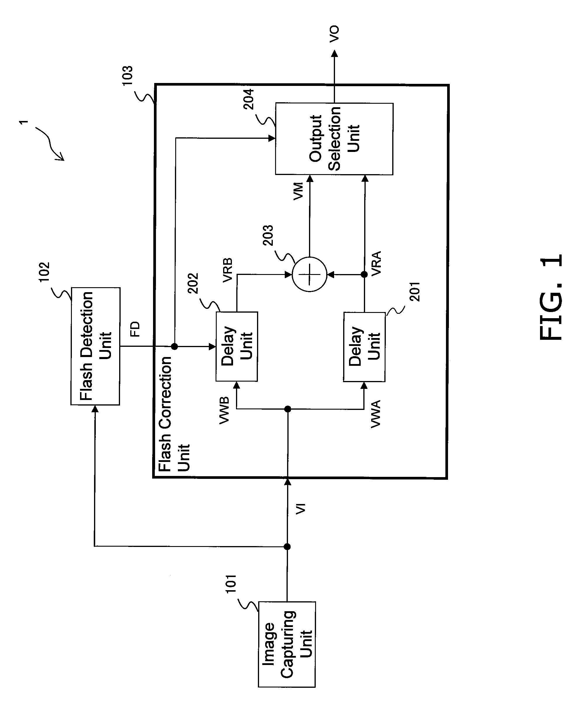
[0078]As shown in FIG. 1, the imaging apparatus 1 includes an image capturing unit 101, a flash detection unit 102, and a flash correction unit 103. The flash c...

second embodiment

[0147]As in the first embodiment, in the second embodiment, the descriptions will be given assuming that the exposure time for a single frame (that is, the accumulation time of a signal charge) is approximately equal to ½ of the signal readout cycle determined by the imaging frame rate (that is, a single frame interval). For example, in the case where the imaging frame rate is 24 frames per second and both one frame interval and the signal readout cycle are 1 / 24 second, the exposure time is 1 / 48 second. Note, however, that unlike the first embodiment, the signal charge readout period is assumed to be 1 / 120 second.

[0148]Furthermore, in the present embodiment, elements that are identical to those of the first embodiment are assigned the same reference numerals, and detailed descriptions thereof will be omitted.

[0149]

[0150]FIG. 5 is a diagram illustrating the overall configuration of an imaging apparatus 2 according to the present embodiment.

[0151]As shown in FIG. 5, the imaging appara...


PUM


Abstract

In the case where a subject is captured by an imaging apparatus that employs a CMOS image sensor, white band interference appears in the captured signal due to the influence of rolling shutter operations when an external flash such as a camera flash has occurred; the present technique obtains an image in which that interference has been corrected even during electronic shutter imaging.An image capturing unit outputs both a valid video signal (a primary video signal) and an unnecessary video signal (a secondary video signal) as an output signal; a flash detection unit detects white band interference caused by an external flash; and a flash correction unit delays the valid video signal using a first delay unit and delays the unnecessary video signal using a second delay unit. When white band interference has occurred, the outputs of the respective delay units are added together by an adding unit, generating a corrected signal. An output selection unit selects and outputs the signal from the first delay unit in normal times, and when interference caused by an external flash has occurred, selects and outputs the corrected signal.

Description

CROSS-REFERENCE TO RELATED APPLICATION[0001]This application claims priority to Japanese Patent Application No 2010-107844 filed on May 10, 2010, the entire disclosure of which is hereby incorporated herein by reference.BACKGROUND[0002]1. Technical Field[0003]The present technique relates to imaging apparatuses capable of reducing white band interference arising when the flash of a still camera or the like (an external flash) occurs when capturing a moving picture for a video.[0004]2. Description of the Related Art[0005]In recent years, imaging apparatuses that use CMOS (Complementary Metal Oxide Semiconductor) image sensors, which are compact, consume little power, capture images at high speeds, and so on, are being employed in the fields of consumer video cameras and professional video cameras.[0006]A CMOS image sensor has various properties that are different from a CCD (Charge Coupled Device) image sensor, and the method for reading out charges accumulated in a photodiode (also ...

Claims


Application Information

Patent Timeline
IPC IPC(8): H04N5/262
CPCH04N23/56H04N23/71H04N25/531H04N23/74
Inventor FUKUSHIMA, YASUSHI
Owner PANASONIC CORP
Why Eureka
Try Eureka