Mitigating channel coupling effects during sensing of non-volatile storage elements

Active Publication Date: 2011-11-10
SANDISK TECH LLC
View PDF4 Cites 29 Cited by
  • Summary
  • Abstract
  • Description
  • Claims
  • Application Information

AI Technical Summary

Problems solved by technology

However, differences in the neighbor's channel potential between when the memory cell was verified and later read can impact the apparent Vt of the memory cell.
Because m

Method used


Image

  • Mitigating channel coupling effects during sensing of non-volatile storage elements
  • Mitigating channel coupling effects during sensing of non-volatile storage elements
  • Mitigating channel coupling effects during sensing of non-volatile storage elements

Examples


Embodiment Construction

[0041]Techniques are disclosed for improvements in operating non-volatile storage devices. The amount of channel coupling that a specific memory cell experiences from one or more neighbor memory cells during read may be matched to the amount of channel coupling that occurred from the neighbor(s) during verify. Therefore, differences in channel coupling between program verify and read are reduced or eliminated.

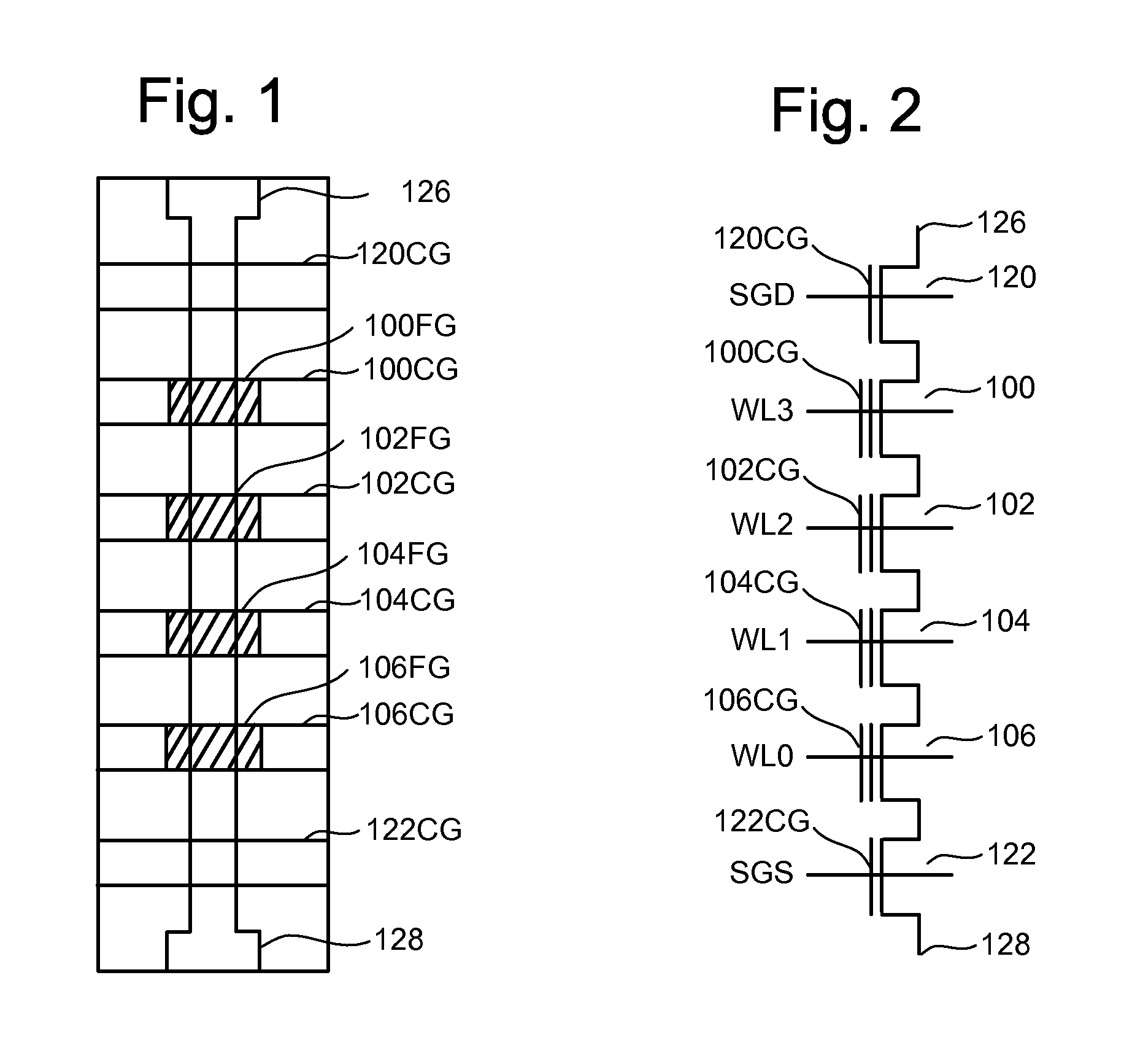
[0042]Note that the threshold voltage of the target memory cell being sensed may depend on the bit line bias of the neighbor memory cells. For example, if the neighbor's bit line is grounded, the threshold voltage of the target memory may be higher than if the neighbor's bit line is biased at Vbl (where Vbl may be, for example, 0.4V). On the other hand, if the neighbor's bit line is biased at Vbl, the threshold voltage of the target memory cell may be lower than if the neighbor's bit line is grounded. Embodiments include methods and devices that match the bit line bias conditio...


PUM


Abstract

Channel coupling effects during verify and read of non-volatile storage are mitigated by matching the amount of channel coupling that occurs during read with channel coupling that occurred during verify. All bit lines may be read together during both verify and read. In one embodiment, first bias conditions are established on bit lines when verifying each of a plurality of programmed states. A separate set of first bias conditions may be established when verifying each state. Biasing a bit line may be based on the state to which a non-volatile storage elements on the bit line is being programmed. A separate set of second bias conditions are established for each state being read. The second bias conditions for a given state substantially match the first bias conditions for the given state.

Description

BACKGROUND[0001]1. Field of the Invention[0002]This disclosure relates to non-volatile storage.[0003]2. Description of the Related Art[0004]Semiconductor memory has become more popular for use in various electronic devices. For example, non-volatile semiconductor memory is used in personal navigation devices, cellular telephones, digital cameras, personal digital assistants, mobile computing devices, non-mobile computing devices and other devices. Electrical Erasable Programmable Read Only Memory (EEPROM) and flash memory are among the most popular non-volatile semiconductor memories.[0005]In both EEPROM and flash memory, a memory cell includes a transistor with a floating gate that is positioned above and insulated from a channel region in a semiconductor substrate. The floating gate and channel regions are positioned between the source and drain regions. A control gate is provided over and insulated from the floating gate. The threshold voltage of the transistor is controlled by t...

Claims


Application Information

Patent Timeline
IPC IPC(8): G11C16/06
CPCG11C16/3418G11C11/5642
Inventor DONG, YINGDALI, YANHSU, CYNTHIA
Owner SANDISK TECH LLC
Why Eureka
Try Eureka