Test apparatus and test method

a test apparatus and test method technology, applied in the field of test apparatus and test method, can solve the problems of increasing testing cost and lowering throughpu

Active Publication Date: 2011-11-17
ADVANTEST CORP
View PDF17 Cites 32 Cited by
  • Summary
  • Abstract
  • Description
  • Claims
  • Application Information

AI Technical Summary

Benefits of technology

[0010]Therefore, it is an object of an aspect of the innovations herein to provide a test apparatus and a test method, which are capable of overcoming the above drawbacks accompanying the related art. The above and other objects can be achieved by combinations described in the claims. A first aspect of the innovations may include a test apparatus for testing a device under test, including a test signal generator that generates a test signal to test the device under test, an electric-photo converter that converts the test signal into an optical test si

Problems solved by technology

This, however, lowers the throughput

Method used


Image

  • Test apparatus and test method
  • Test apparatus and test method
  • Test apparatus and test method

Examples


Embodiment Construction

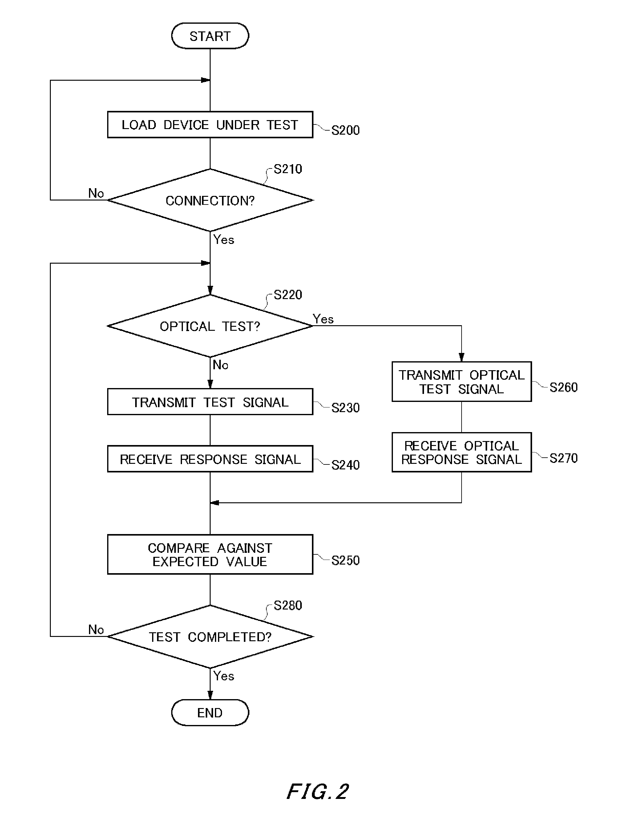
[0018]Hereinafter, some embodiments of the present invention will be described. The embodiments do not limit the invention according to the claims, and all the combinations of the features described in the embodiments are not necessarily essential to means provided by aspects of the invention.

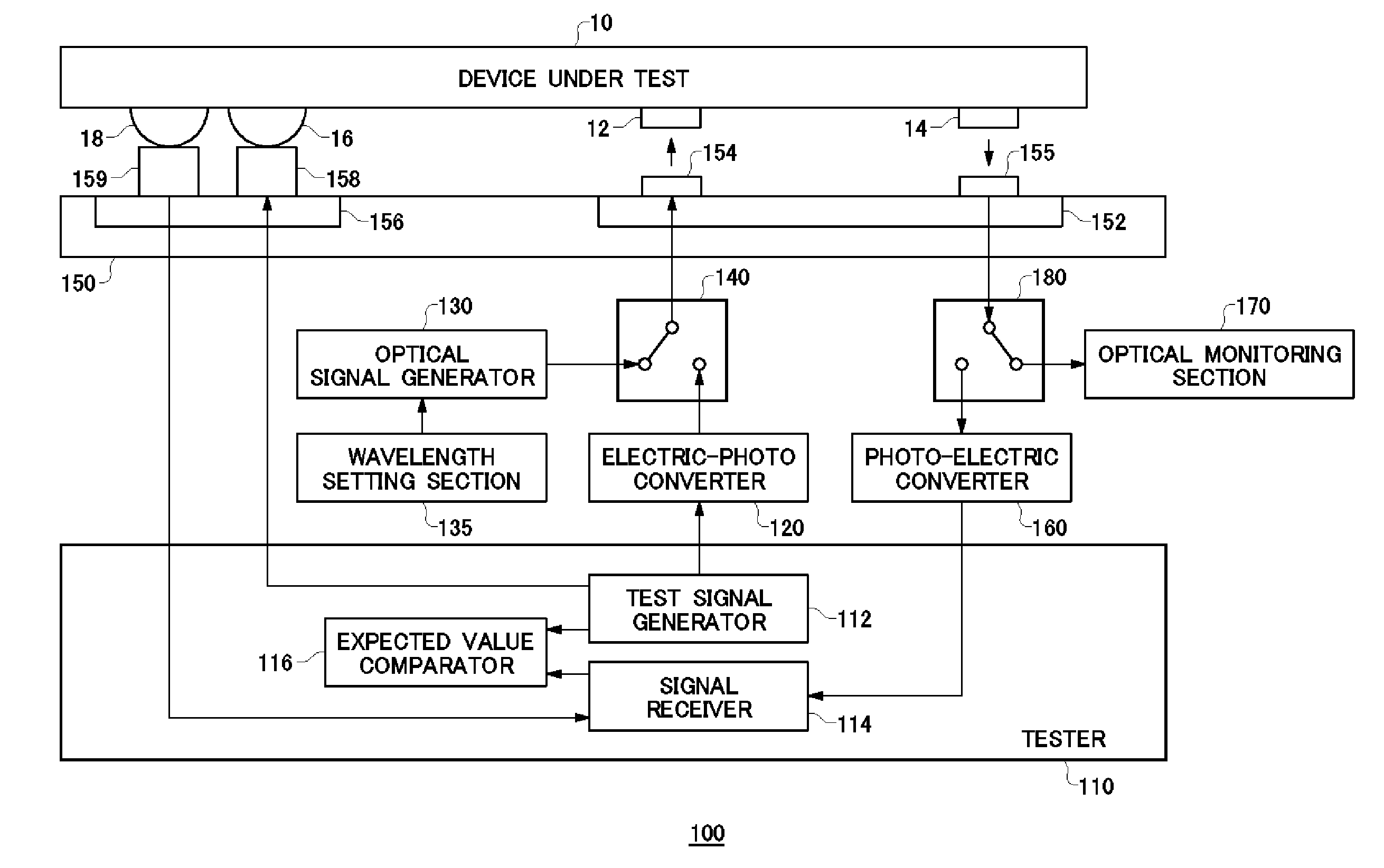
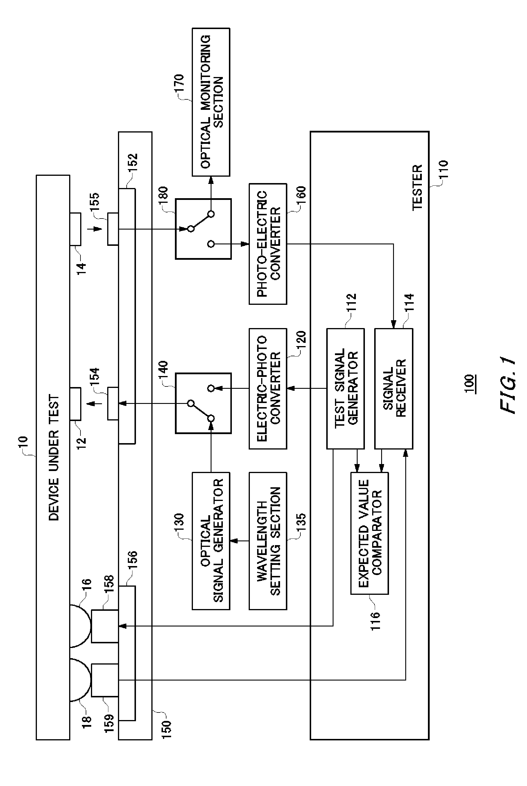
[0019]FIG. 1 illustrates an exemplary configuration of a test apparatus 100 relating to an embodiment of the present invention, together with a device under test 10. The test apparatus 100 is an analog circuit, a digital circuit, a memory, and a system on chip (SOC), and tests the device under test 10 including an optical interface. The device under test 10 may be a circuit having a combination of at least one of an analog circuit, a digital circuit, a memory and a system on chip (SOC) and an optical interface. The device under test 10 has one or more optical receivers 12 and one or more optical transmitters 14 for exchanging optical signals. The device under test 10 may include one or more inp...


PUM


Abstract

There is provided a test apparatus for testing a device under test, including a test signal generator that generates a test signal to test the device under test, an electric-photo converter that converts the test signal into an optical test signal, an optical interface that (i) transmits the optical test signal generated by the electric-photo converter to an optical receiver of the device under test and (ii) receives and outputs an optical response signal output from the device under test, a photo-electric converter that converts the optical response signal output from the optical interface into an electrical response signal and transmits the electrical response signal, and a signal receiver that receives the response signal transmitted from the photo-electric converter and a test method.

Description

BACKGROUND[0001]1. Technical Field[0002]The present invention relates to a test apparatus and a test method.[0003]2. Related Art[0004]A test apparatus has been conventionally designed to test a device under test such as a CPU and a memory. A loopback test has been proposed that is used to test a device under test at an actual operation speed, for example, as disclosed in Patent Document 1. It has been also proposed to provide a device under test with an optical interface, for example, as disclosed in Patent Document 2.[0005]Patent Document 1: Japanese Patent Application Publication No. 2006-220660[0006]Patent Document 2: International Publication No. 2007-013128[0007]Non-Patent Document 1: Ian A. Young, et al., “Optical I / O Technology for Tera-Scale Computing”, IEEE Journal of Solid-State Circuits, January 2010, Vol. 45, No. 1, pp.235-248[0008]Non-Patent Document 2: Hiren D. Thacker, James D. Meindl, “Prospects for Wafer-Level Testing of Gigascale Chips with Electrical and Optical I...

Claims


Application Information

Patent Timeline
IPC IPC(8): G01R31/00
CPCG01R31/2889G01R31/31728G01R31/31917G01R31/3025
Inventor MASUDA, SHIN
Owner ADVANTEST CORP
Why Eureka
Try Eureka