Semiconductor module with electrical switching elements

Active Publication Date: 2011-12-01
DENSO CORP
View PDF2 Cites 44 Cited by
  • Summary
  • Abstract
  • Description
  • Claims
  • Application Information

AI Technical Summary

Benefits of technology

[0032]Hence, this allows four switching elements to be located closer to each other. Inductance caused between these four switching elements can be red

Problems solved by technology

This results in a rise in manufacturing cost of the power conversion apparatus 90.
However, a conventional semiconductor module has a snubber capacitor wire-bonded, so that the

Method used


Image

  • Semiconductor module with electrical switching elements
  • Semiconductor module with electrical switching elements
  • Semiconductor module with electrical switching elements

Examples


first embodiment

[0050]Referring to FIGS. 2 to 7, the first embodiment of the semiconductor module according to the present invention will now be described.

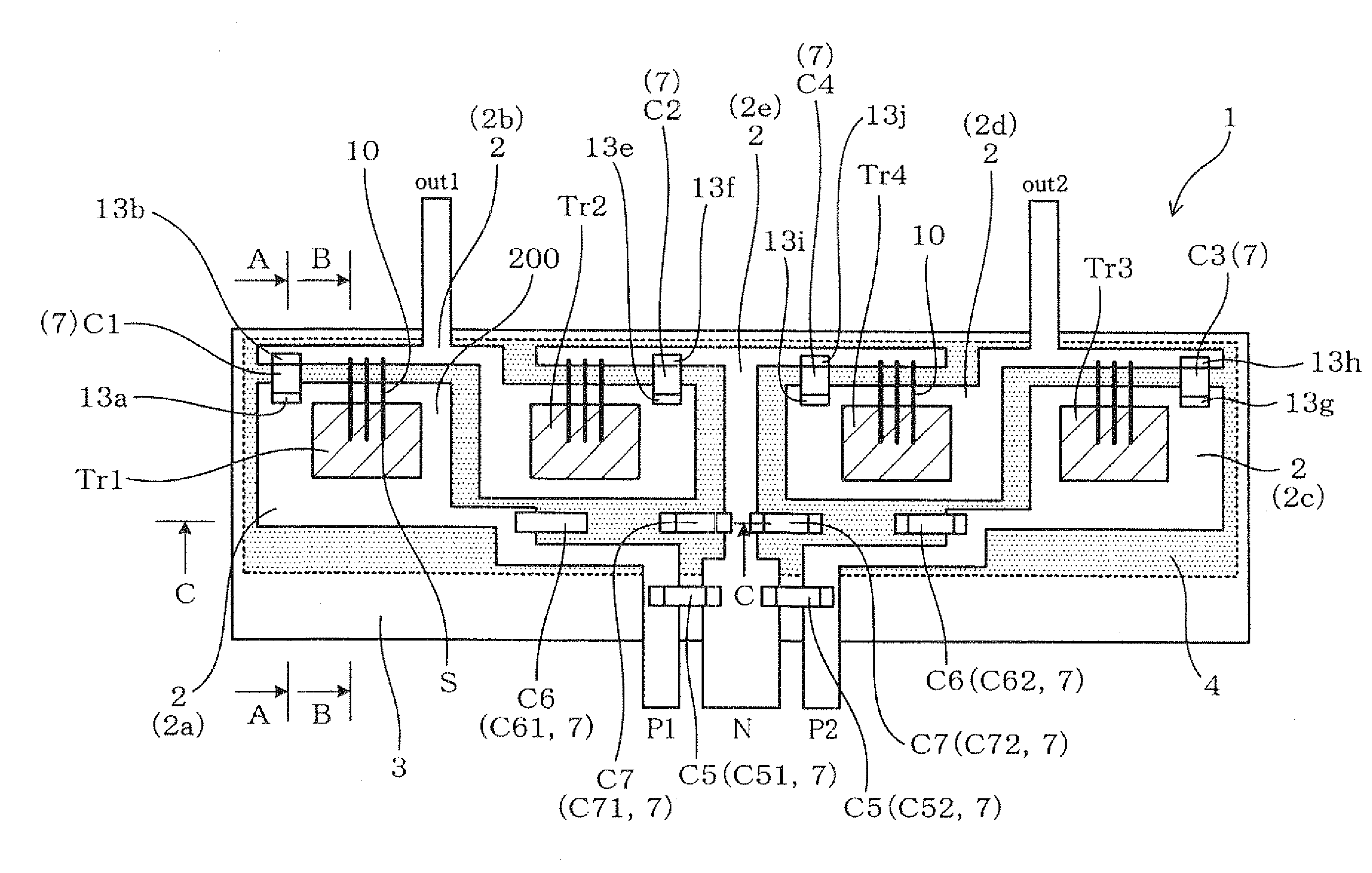
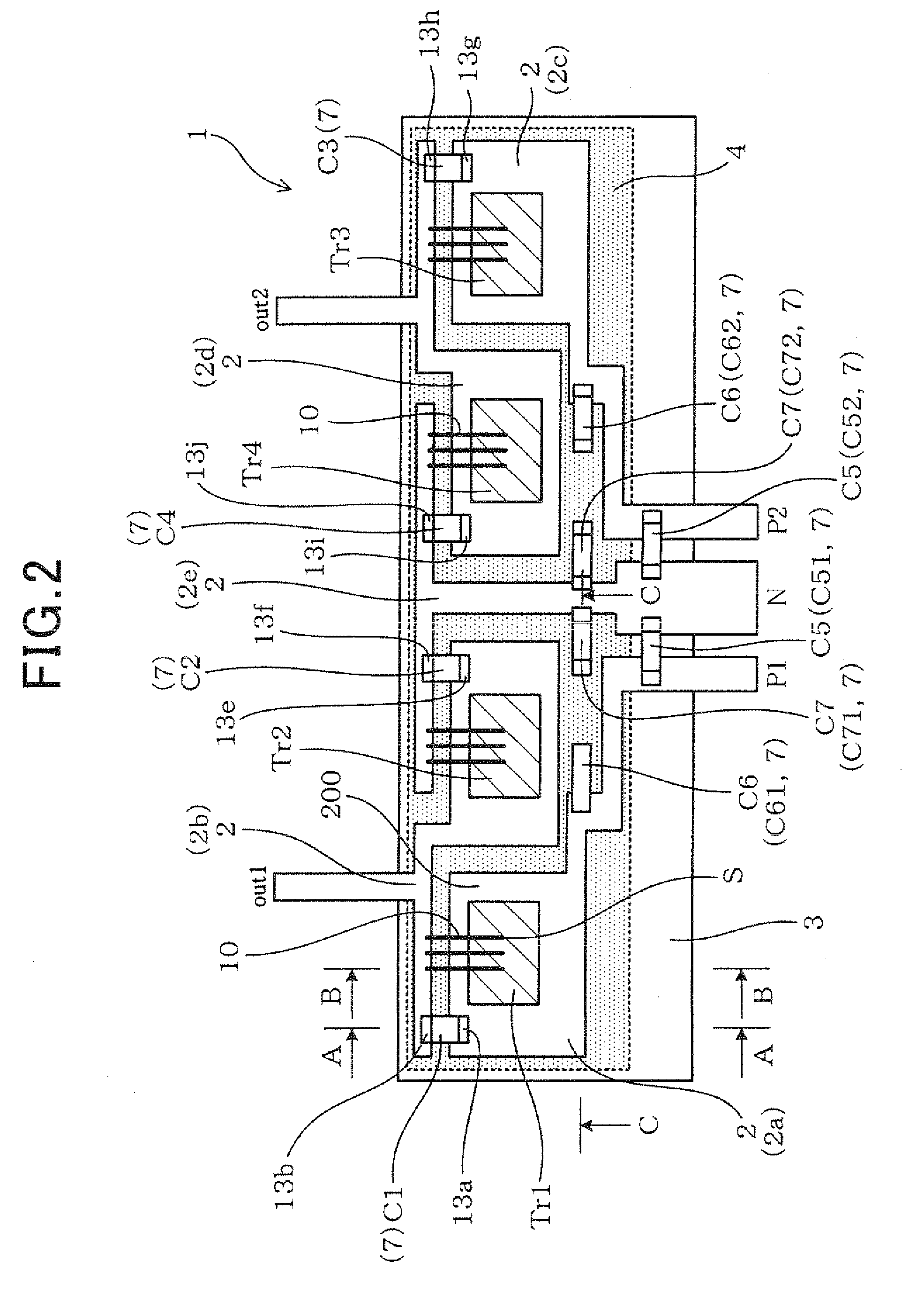
[0051]As shown in FIG. 2, a semiconductor module 1 according to the present invention has a plurality of lead frames 2, switching elements Tr (Tr1 to Tr4), electronic components 7, and a sealing member 3.

[0052]Each of the switching elements Tr is electrically connected to a corresponding one of the lead frames 2. The electronic components 7 are electrically connected to the switching elements Tr. The sealing member 3 seals part of the lead frames 2, the switching elements Tr1 to Tr4, and the electronic components 7.

[0053]As shown in FIGS. 2 and 3, the electronic components are mounted on the primary surface 200 of the respective lead frames 2.

[0054]As shown in FIG. 2, the semiconductor module 1 has five lead frames 2a to 2e. To each of the first to fourth lead frames 2a to 2d, a single switching element Tr is connected. The switching elements Tr1...

second embodiment

[0085]Referring to FIG. 8, a semiconductor module according to a second embodiment of the present invention will now be described.

[0086]In the second embodiment and subsequent embodiments, the same or identical components as or to those employed in the first embodiment, the same reference numerals are given for the sake of a simplified or omitted explanation.

[0087]The present embodiment provides an example in which the number of switching element groups 6 incorporated in the single semiconductor module 1 is changed from the foregoing one. As shown in FIG. 8, the embodiment shows that only one switching element group 6 is sealed for modularization.

[0088]This embodiment is thus preferable to an electronic circuit which requires only a single switching element group 6. In comparison with the foregoing configuration in which the plural switching element groups 6 are united, the electronic circuit can be produced with less cost, because only one switching element group 6 is needed.

[0089]...

third embodiment

[0090]Referring to FIG. 9, a semiconductor module according to a third embodiment of the present invention will now be described.

[0091]The present embodiment provides an example in which the line bypass capacitors C6 and C7 are connected to the ground terminal 4 in another way. As shown in FIG. 9, the ground terminal 4 has no protrusion which is different from the protrusion 40 shown in FIG. 5, and is flat. The ground terminal 4 has the primary surface 400 on which a metal block 41 with a primary surface 410 is mounted and soldered or welded. The primary surfaces 200 of the lead frames 2 are approximately equal in level to the primary surface 410 of the metal block 41. The line bypass capacitors C6 and C7 are mounted to bridge over each of the lead frames 2 and the metal block 41, and soldered and welded.

[0092]The remaining configurations are identical to those described in the first embodiment.

[0093]The advantages of the present invention are as follows. The ground terminal 4 is no...


PUM


Abstract

A semiconductor module is provided which is capable of lowering surges caused when switching elements are switched on and off. The module has a plurality of lead frames, switching elements, electronic components, and a sealing member. The switching elements are electrically connected to the lead fames respectively. Part of the lead frames, the switching elements, and the electronic components are sealed by the sealing member. The electronic components are mounted on primary surfaces of the lead frames respectively.

Description

CROSS REFERENCE TO RELATED APPLICATIONS [0001]This application is based on and claims the benefit of priority from earlier Japanese Patent Application Nos. 2010-92744 filed Apr. 14, 2010 and 2011-85974 filed Apr. 8, 2011, the description of which is incorporated herein by reference.BACKGROUND OF THE INVENTION[0002]1. (Technical Field)[0003]The present invention relates to a semiconductor module provided with electronic components, and in particular, to a semiconductor module provided with switching elements which serve as electronic components.[0004]2. (Related Art)[0005]There have been known power conversion apparatuses mounted in vehicles. Such apparatuses include apparatuses described by Japanese Patent Laid-open Publication Nos. 2000-333476 and 2008-136333.[0006]The power conversion apparatus described in these publications has a configuration shown in FIG. 1. Practically, as shown, a power conversion apparatus 90 has a semiconductor module 900 including switching semiconductors...

Claims


Application Information

Patent Timeline
IPC IPC(8): H01L29/02H01L23/495
CPCH01L23/49537H01L23/49541H01L23/49562H01L23/49575H01L23/49589H01L2224/48247H01L2924/3011H01L24/48H01L2924/19105H01L2924/30107H01L2924/13091H01L2924/13055H01L2924/00H01L2924/181H01L2224/4903H01L2224/49175H01L2224/73265H01L2924/00014H01L2224/48091H01L24/49H01L2224/0603H01L2224/49111H01L23/642H01L2924/00012H01L2224/45099H01L2224/45015H01L2924/207
Inventor HAYASHI, YUJIHANDA, YUUICHI
Owner DENSO CORP
Why Eureka
Try Eureka