

Display device
- Summary
- Abstract
- Description
- Claims
- Application Information
AI Technical Summary
Benefits of technology
Problems solved by technology
Method used
Image

Examples
example
[0062]Aspects of the present invention are further described below with reference to an example. The present invention is not limited to the example.
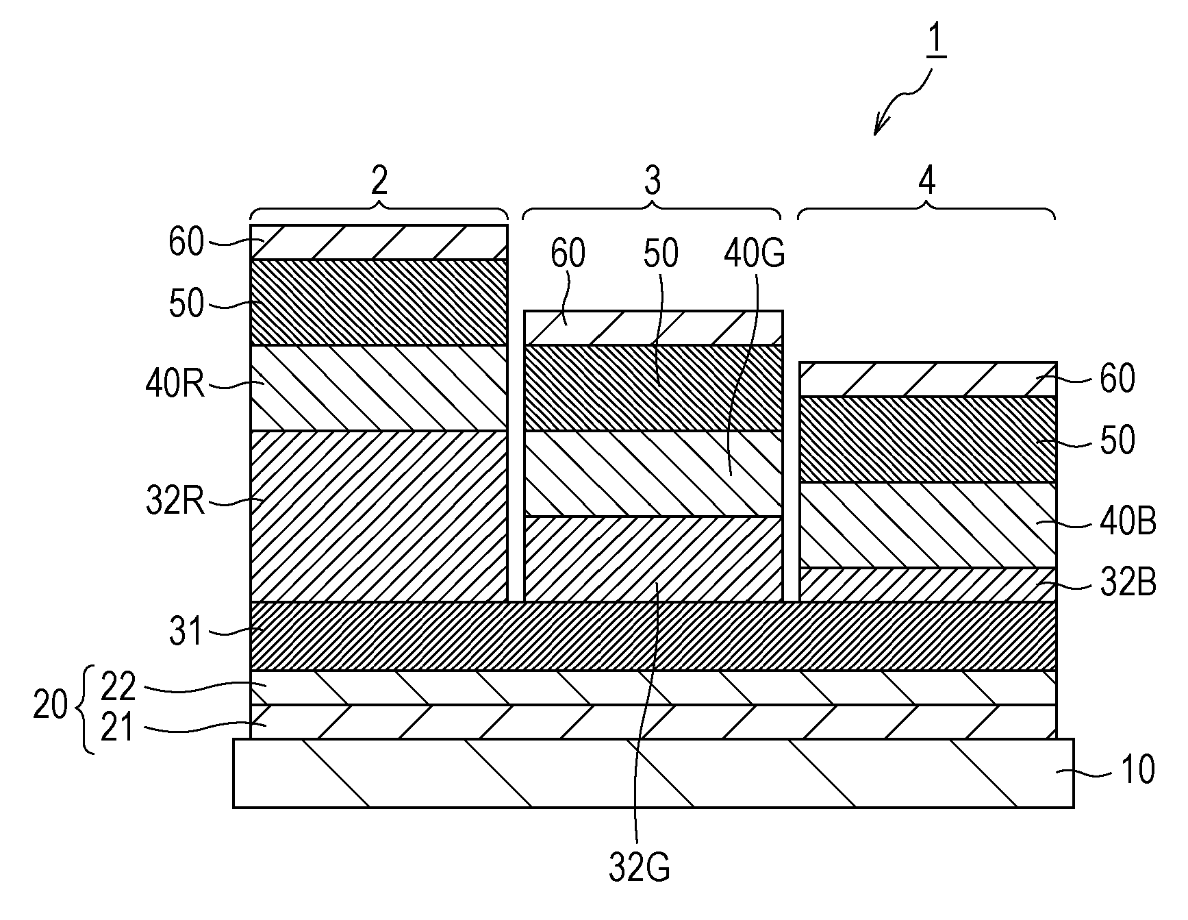
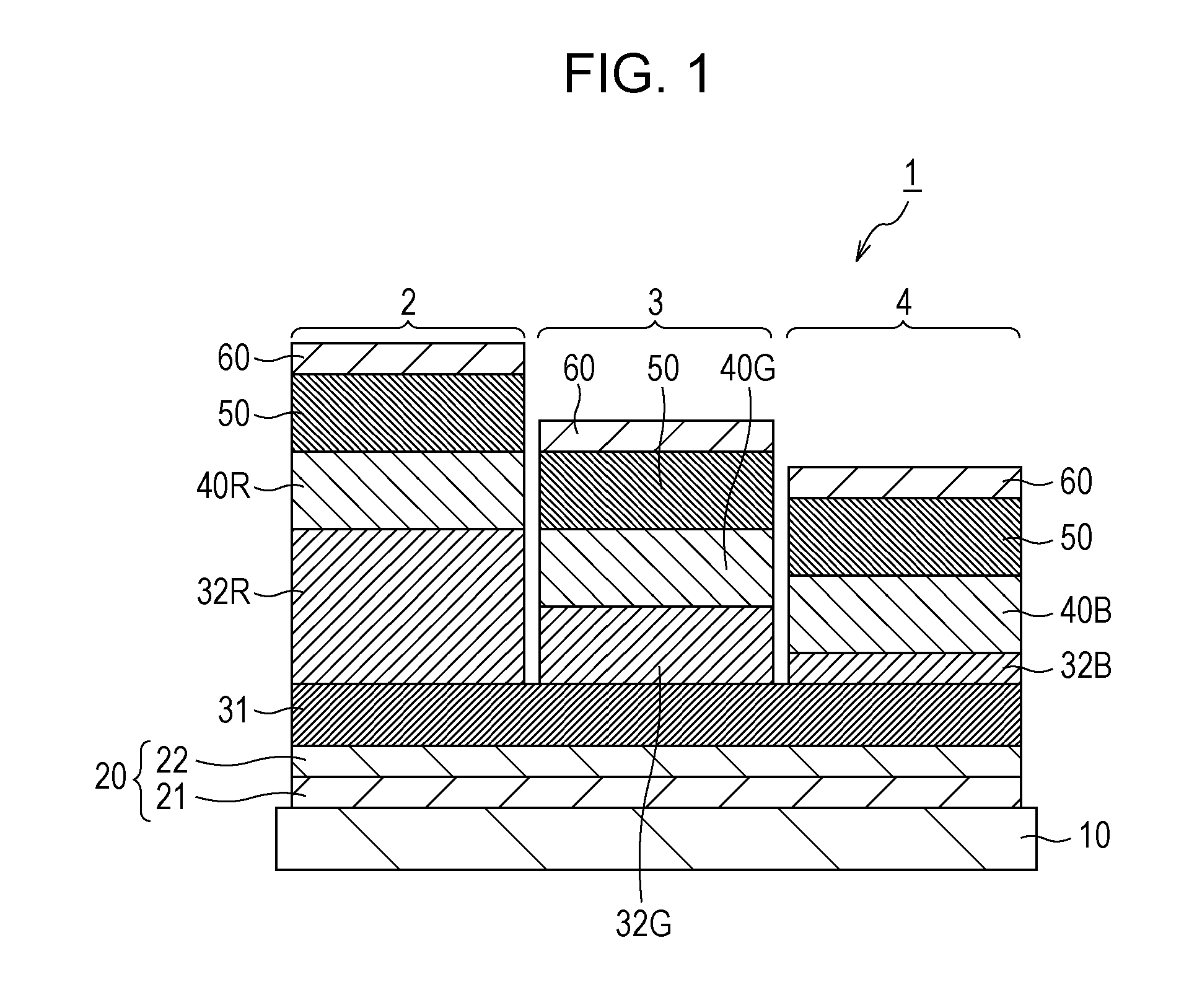
[0063]A display device shown in FIG. 1 was prepared by a procedure below.
[0064]A layer of an aluminum alloy (Al—Nd) was deposited on a glass substrate (substrate 10) by a sputtering process, whereby a reflective sub-electrode (reflective sub-anode) 21 was formed. The reflective sub-electrode 21 had a thickness of 100 nm. A layer of ITO was deposited on the reflective sub-electrode 21 by a sputtering process, whereby a transparent sub-electrode (transparent sub-anode) 22 was formed. The transparent sub-electrode 22 had a thickness of 38 nm. The reflective sub-electrode 21 and the transparent sub-electrode 22 collectively functioned as a first electrode (anode) 20. A polyimide film was formed on the substrate 10 having the first electrode 20 and was then patterned, whereby a pixel separator (not shown) was formed. The pixel separator had ...
PUM
 Abstract
Description
Claims
Application Information