Photoelectrical element having a thermal-electrical structure

a photoelectrical element and thermal-electrical technology, applied in the field of photoelectrical elements, can solve the problems of reducing the recombination rate of electrons and holes, not spreading current well, and affecting the electrical performance of the element,

Active Publication Date: 2011-12-08
EPISTAR CORP
View PDF1 Cites 0 Cited by
  • Summary
  • Abstract
  • Description
  • Claims
  • Application Information

AI Technical Summary

Problems solved by technology

Now, the LED generally has the problem, which is the current spreading not well.
Otherwise, the LED also has the heat dissipation problem.
When the temper

Method used


Image

  • Photoelectrical element having a thermal-electrical structure
  • Photoelectrical element having a thermal-electrical structure
  • Photoelectrical element having a thermal-electrical structure

Examples


Embodiment Construction

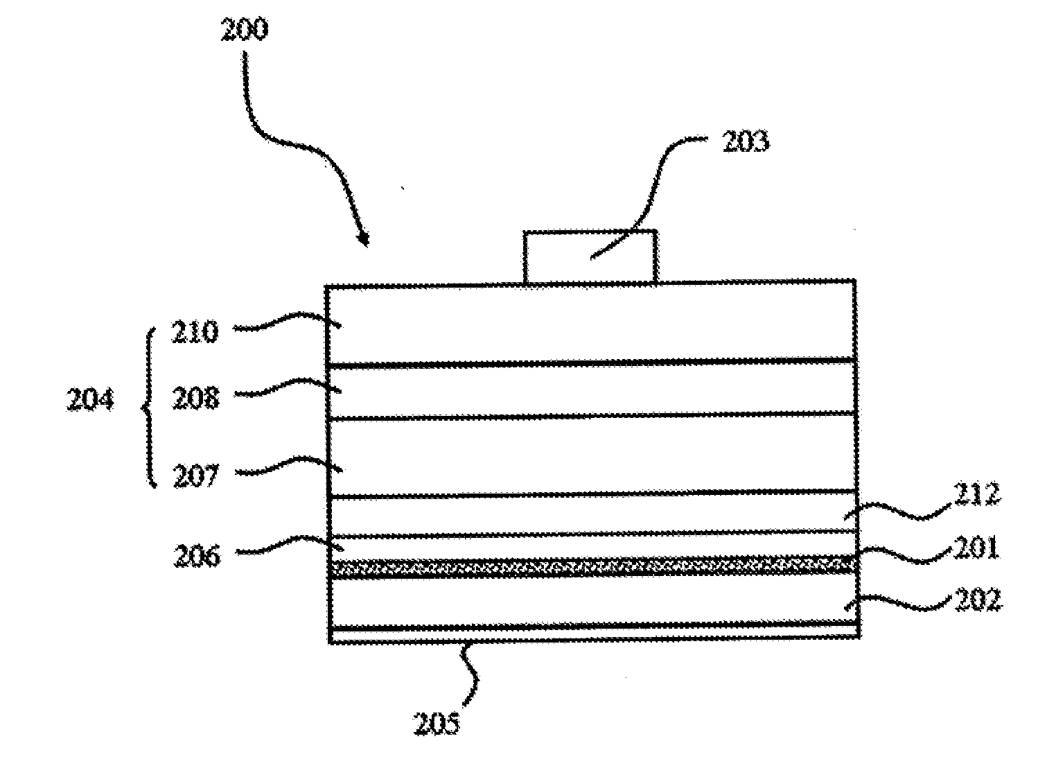
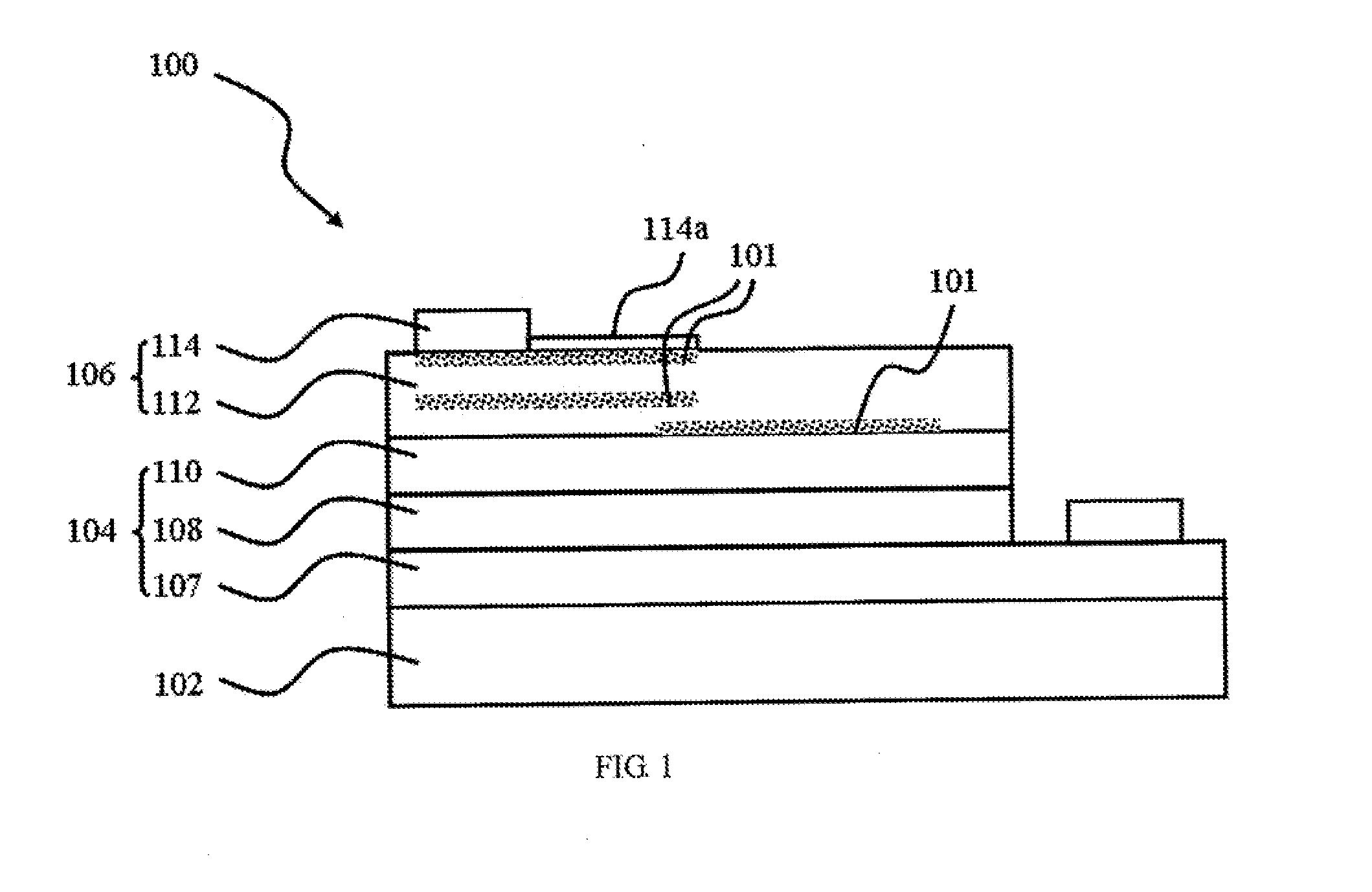
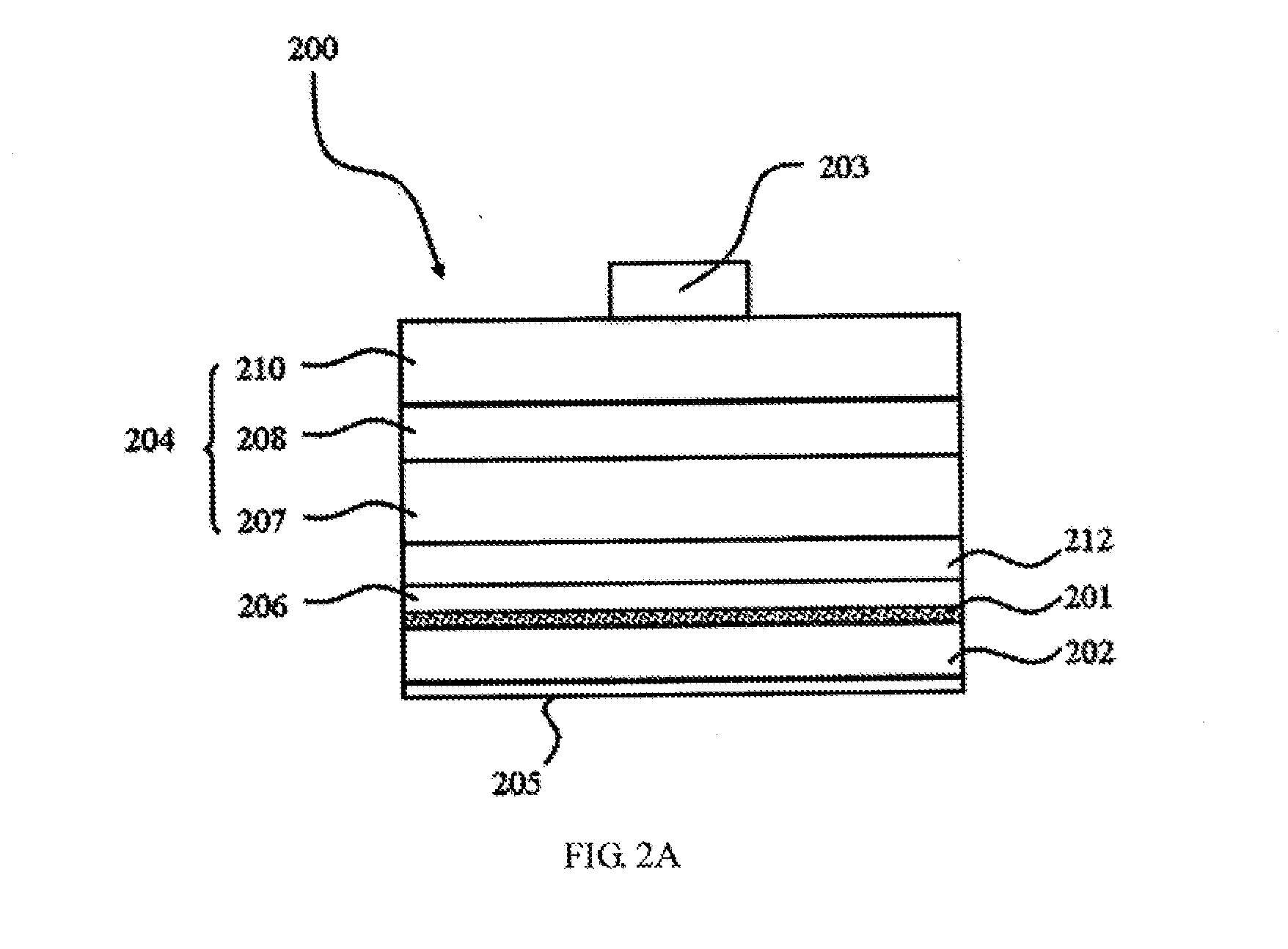
As shown in FIG. 1, a photoelectrical element 100 illustrated in the first embodiment of the present application comprises: a substrate 102; a photoelectric conversion stacked-layer 104 formed on the substrate 102; a conductive structure 106 formed on the photoelectric conversion stacked-layer 104; and a thermal-electrical structure 101 formed inside the conductive structure 106. The photoelectric conversion stacked-layer 104 comprises a first semiconductor layer 107 formed on the substrate 102, a photoelectric conversion layer 108 formed on the first semiconductor layer 107, and a second semiconductor layer 110 formed on the photoelectric conversion layer 108, wherein the first semiconductor layer 107 may be the n-type semiconductor layer, the second semiconductor layer 110 may be the p-type semiconductor layer, and the photoelectric conversion layer 108 is used to emit the light. The photoelectrical element 100 of the embodiment is a light emitting element, or a solar cell when th...


PUM


Abstract

A photoelectrical element having a thermal-electrical structure including: a photoelectrical transforming layer, two semiconductor layers formed on the two opposite sides of the photoelectrical transforming layer respectively, an electrically conductive structure formed on at least one of the semiconductor layer, and a thermal-electrical structure formed in the electrically conductive structure, wherein the thermal-electrical structure performs the thermal-electrical transformation to promote current spreading effect, or proceed electrical-thermal transformation to dissipate the heat from the photoelectrical transforming layer.

Description

TECHNICAL FIELDThe present application relates to a photoelectrical element, and in particular, to a photoelectrical element comprising a thermal-electrical structure.REFERENCE TO RELATED APPLICATIONThis application claims the right of priority based on Taiwan application Serial No. 099118367, filed on Jun. 4, 2010, and the content of which is hereby incorporated by reference.DESCRIPTION OF BACKGROUND ARTThe photoelectrical elements include many types such as the light-emitting diode (LED), the solar cell, and the photo diode. Take the LED as an example, the LED is a kind of the solid state semiconductor device, which at least comprises a p-n junction formed between the p-type and the n-type semiconductor layers. When a bias is applied to the p-n junction, the holes of the p-type semiconductor layer combine with the electrons of the n-type semiconductor layer to emit the light. The region where the light is emitted from is called the light-emitting region.Now, the LED generally has ...

Claims


Application Information

Patent Timeline
IPC IPC(8): H01L33/60H01L31/0232
CPCH01L31/022425H01L31/075H01L33/42H01L31/056H01L2933/0075Y02E10/52Y02E10/548H01L33/647
Inventor HSU, MING-CHI
Owner EPISTAR CORP
Why Eureka
Try Eureka