Solid state device and light-emitting element

a technology of solid state devices and light-emitting elements, which is applied in the direction of lighting support devices, instruments, lighting and heating apparatus, etc., can solve the problems of time-consuming and costly bump formation, inability to realize solid state devices having sufficient sealing properties, and inability to achieve sufficient sealing properties. , the effect of reducing the number of bump formations

Active Publication Date: 2006-03-09
TOYODA GOSEI CO LTD
View PDF10 Cites 63 Cited by
  • Summary
  • Abstract
  • Description
  • Claims
  • Application Information

AI Technical Summary

Benefits of technology

[0022] It is a further object of the present invention to provide a solid state device which is excellent in solid state component packaging, sealing, electrical connection, and thermal dissipation.
[0023] It is a still further object of the present invention to provide an LED element and a light-emitting device, the packaging process of which can be simplified.
[0039] According to the present invention, it is possible to realize a solid state device having the sufficient sealing property when using a sealing material made of low melting point glass.
[0040] According to the present invention, it is possible to provide a solid state device which is excellent in solid state component packaging, sealing, electrical connection, and thermal dissipation.
[0041] According to the LED element and the light-emitting device of the present invention, since in the element fabrication process the fusion-bonded portion is electrically connected to the n-side and p-side of the LED element so as to be formed integrally with the LED element, the mounting process can be simplified.

Problems solved by technology

Particularly, in the case of use of group III nitride-based compound semiconductor light-emitting elements which emit short-wavelength light, light-transmitting resin around the elements is caused to turn yellow by high-energy light emitted from the elements and heat produced by the elements themselves, which often unnegligibly degrades efficiency of deriving light.
According to conventional solid state devices, however, because of high viscosity of conventional low melting point glass in a practical sealing temperature range, it is impossible to realize a solid state device having the sufficient sealing property when using a sealing material made of low melting point glass.
This requires time-consuming and costly bump formation.
Particularly, in large-size LED elements, a plurality of stud bumps are arranged for multipoint joining, which can therefore be more significantly time-consuming and costly.
In the above-mentioned bump formation method, however, because the bumps for mounting components have to be formed by photolithography, the number of fabrication steps increases, which results in a high cost.

Method used


Image

  • Solid state device and light-emitting element
  • Solid state device and light-emitting element
  • Solid state device and light-emitting element

Examples


embodiment 1

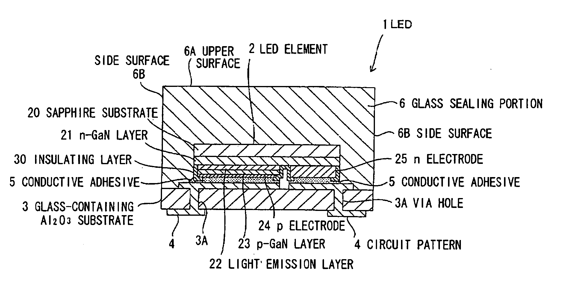
[0063]FIG. 1 is a cross-sectional view illustrating an LED as a solid state device according to a first embodiment of the invention.

[0064] This LED 1 comprises a flip-chip-type LED element 2 made of a GaN-based semiconductor material (thermal expansion coefficient α: 5-7 (×10−6 / ° C.)), a glass-containing Al2O3 substrate 3 as an inorganic material substrate for mounting the LED element 2, a circuit pattern 4 consisting of tungsten (W)-nickel (Ni)-gold (Au) and formed in the glass-containing Al2O3 substrate 3, a conductive adhesive 5 made of Ag paste for electrically connecting the circuit pattern 4 to a p-electrode 24 and an n-electrode 25 of the LED element 2, and a glass sealing portion 6 made of transparent glass bonded to the glass-containing Al2O3 substrate 3 for sealing the LED element 2. In this embodiment, the glass-containing Al2O3 substrate 3 and the circuit pattern 4 form a power receiving / feeding portion, and the joined surfaces of the p-electrode 24 and the n-electrode ...

embodiment 2

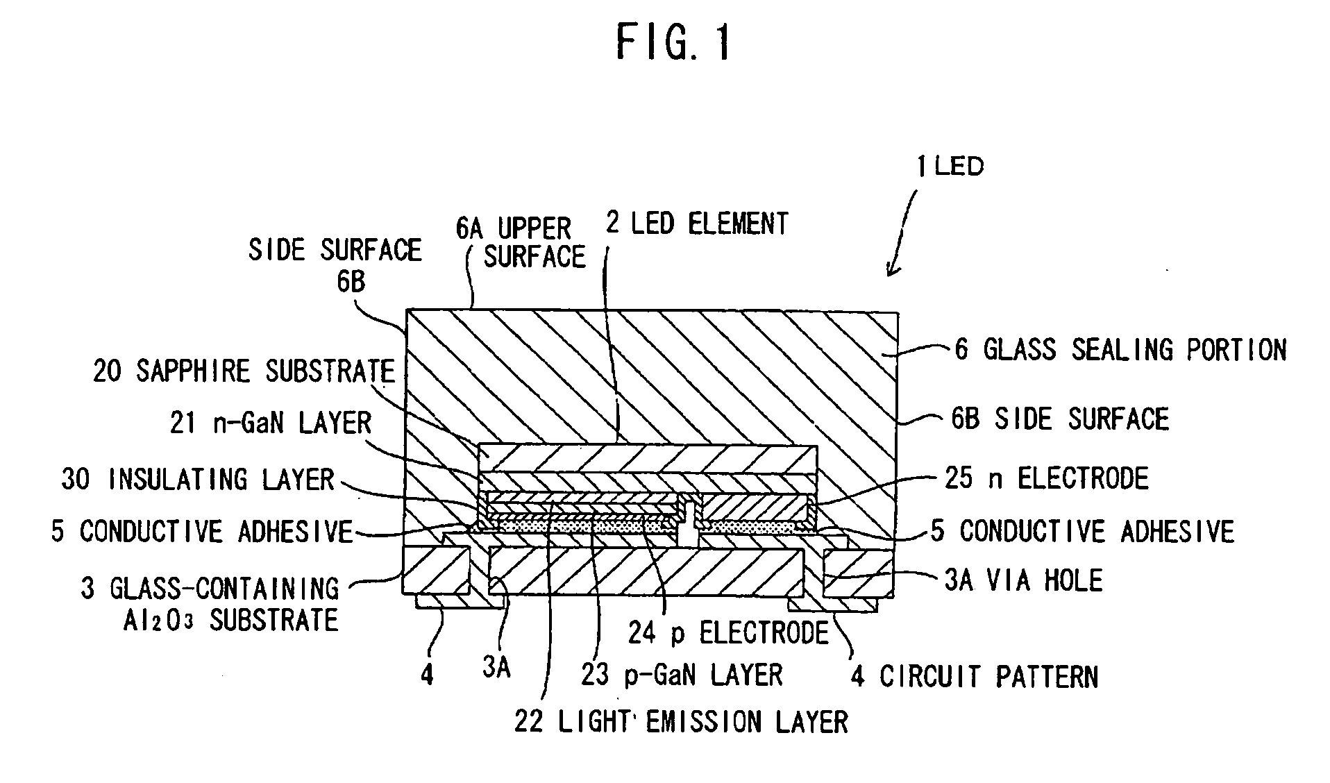
[0089]FIG. 2 is a cross-sectional view illustrating an LED as a solid state device according to a second embodiment of the invention. In the following embodiments, the same reference numbers as those of the first embodiment respectively denote the portions having the same structure and function as those in the first embodiment.

[0090] This LED 1 is different from that of the first embodiment in screen-printing high viscous Ag paste as the conductive adhesive 5 on a portion positioned on the n-electrode 25 of the LED element 2 explained in the first embodiment, and bringing the p-electrode 24 into close contact with the circuit pattern 4 directly without Ag paste therebetween.

[0091] The effects of the second embodiment are as follows.

[0092] (1) Since no internal stress occurs in glass at high temperatures during glass processing, but glass contracts as cooled, which causes compression stress from the glass sealing portion 6 and the sapphire substrate 20 to the LED element 2, the el...

embodiment 3

[0095]FIG. 3 is a cross-sectional view illustrating an LED as a solid state device according to a third embodiment of the invention.

[0096] This LED 1 is different from that of the first embodiment in that, to make possible electrical connection on the element side surfaces and surface mounting on the semiconductor layer side, an LED element 2 with a p-electrode 24 and an n-electrode 25 formed so as to be exposed to element edges from the element side surfaces to p-contact layer 240 surface are mounted on a circuit pattern 4 provided on an Al2O3 substrate 300 (thermal expansion coefficient: 7×10⁻⁶ / ° C.), and sealed with a glass sealing portion 6 made of SiO2—Nb2O5-based low melting point glass. Here, the term “element edges” refers to edges of side surfaces of the LED element 2, and GaN-based semiconductor layer mounting surface formed in an insulating layer 31, as shown in FIG. 3.

[0097] The LED element 2 comprises an AlN buffer layer 200, an n-GaN layer 21, a light-emitting layer ...


PUM


Abstract

A solid-state device having: a flip-chip mounted solid-state element; a power receiving / feeding portion having a mounting substrate to allow that a mounting surface of the solid-state element forms substantially the same plane as a surface of the mounting substrate; and an inorganic sealing portion made of an inorganic sealing material having a thermal expansion coefficient equal to that of the power receiving / feeding portion for sealing the solid-state element.

Description

[0001] The present application is based on Japanese patent application Nos. 2004-263097 and 2004-316007, the entire contents of which are incorporated herein by reference. BACKGROUND OF THE INVENTION [0002] 1. Field of the Invention [0003] The present invention relates to a solid state device, and particularly, to a solid state device which is sealed with a sealing material made of low melting point glass. [0004] The present invention also relates to a light-emitting element made of a semiconductor material and a light-emitting device using the light-emitting element, and particularly, to a light-emitting element and a light-emitting device which are flip-chip mounted. [0005] Herein, a solid state device includes various optical devices or elements such as a light-emitting device or element, a light-receiving device or element, and a solar cell. Also, herein, a light-emitting element includes an LED element, and a light-emitting device includes an LED. [0006] 2. Description of the R...

Claims


Application Information

Patent Timeline
Patent Type & Authority Applications(United States)
IPC IPC(8): H01L31/00H01L33/08H01L33/38H01L33/48H01L33/56
CPCH01L23/3121H01L31/0203H01L33/08H01L33/38H01L33/486H01L33/56Y10S362/80H01L2924/01078H01L2924/01079H01L2924/09701H01L2924/01322H01L2924/12041H01L2224/16H01L2224/0554H01L2224/05568H01L2224/05573H01L2224/05624H01L2224/0615H01L2924/00014H01L2924/181H01L2924/00012H01L2224/05599H01L2224/0555H01L2224/0556
Inventor SUEHIRO, YOSHINOBUICHIKAWA, MASAYOSHIWADA, SATOSHITASUMI, KOJI
Owner TOYODA GOSEI CO LTD
Why Eureka
Try Eureka