Single-gate finfet and fabrication method thereof

a technology of single-gate fins and fins, applied in the direction of basic electric elements, electrical apparatus, semiconductor devices, etc., can solve the problems of word line spacing, difficulty in frequently encountered, and the difficulty of dram manufacturers to shrink memory cell area, etc., to solve or eliminate the electrical coupling effect

Inactive Publication Date: 2011-12-08
NAN YA TECH
View PDF2 Cites 33 Cited by
  • Summary
  • Abstract
  • Description
  • Claims
  • Application Information

AI Technical Summary

Benefits of technology

[0007]The present invention aims at resolving or eliminating the electrical coupling effect of the advanced DRAM device, which stems from the continuing scaling of the word line spacing and other shrinking rules of the DRAM device.

Problems solved by technology

However, difficulties are frequently encountered in attempting to produce the vast arrays of vertical double-gate FinFET devices desired for semiconductor DRAM applications while maintaining suitable performance characteristics of the devices.
For example, recently DRAM manufacturers face a tremendous challenge on shrinking the memory cell area as the word line spacing, i.e., the spacing between two adjacent word lines, continues to shrink.
The shrinking spacing between two closely arranged word lines leads to undesirable electrical coupling effect for high-speed DRAM applications.
Another drawback of the prior art transistor structure is insufficient source / drain contact landing area.

Method used


Image

  • Single-gate finfet and fabrication method thereof
  • Single-gate finfet and fabrication method thereof
  • Single-gate finfet and fabrication method thereof

Examples


Embodiment Construction

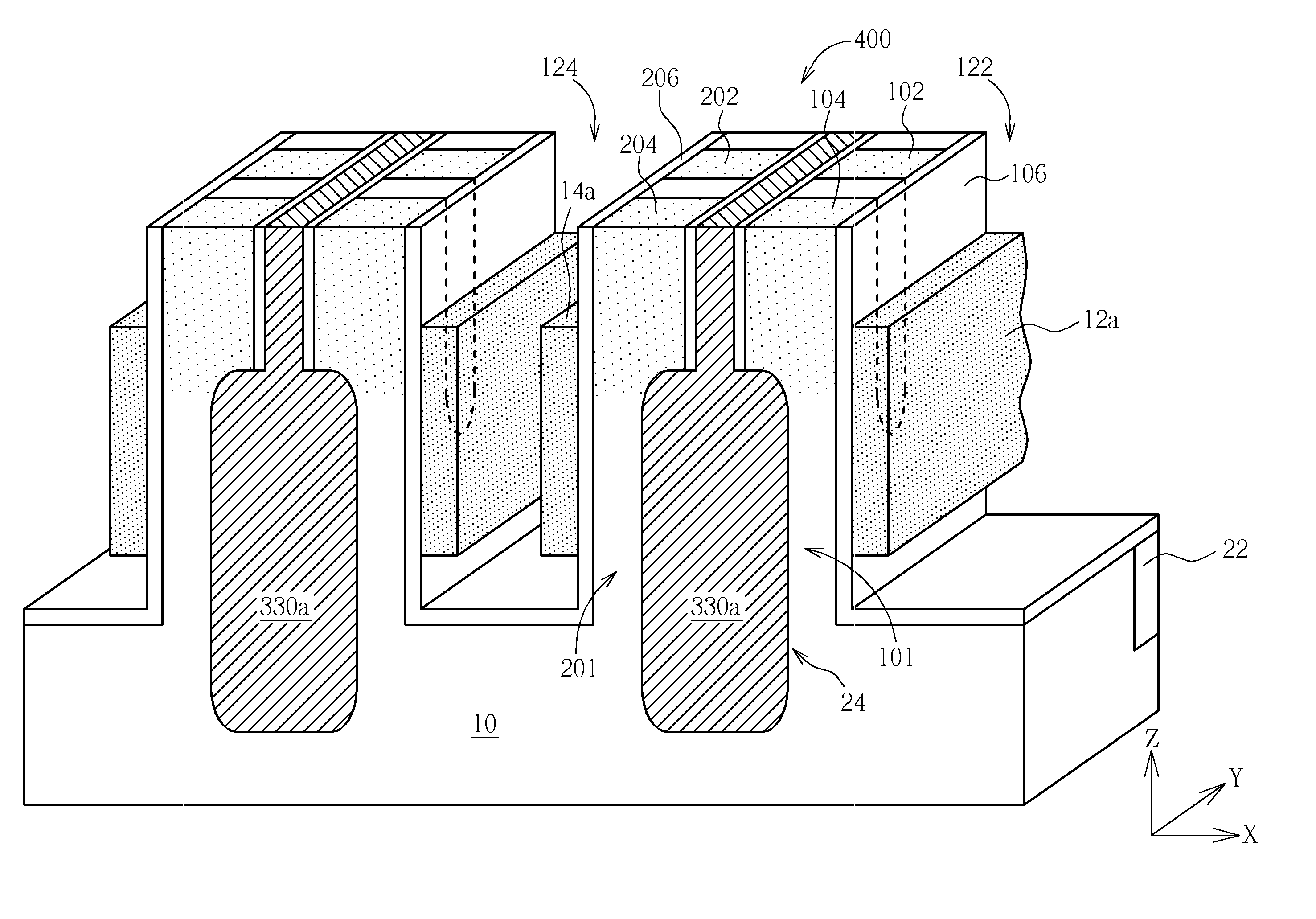
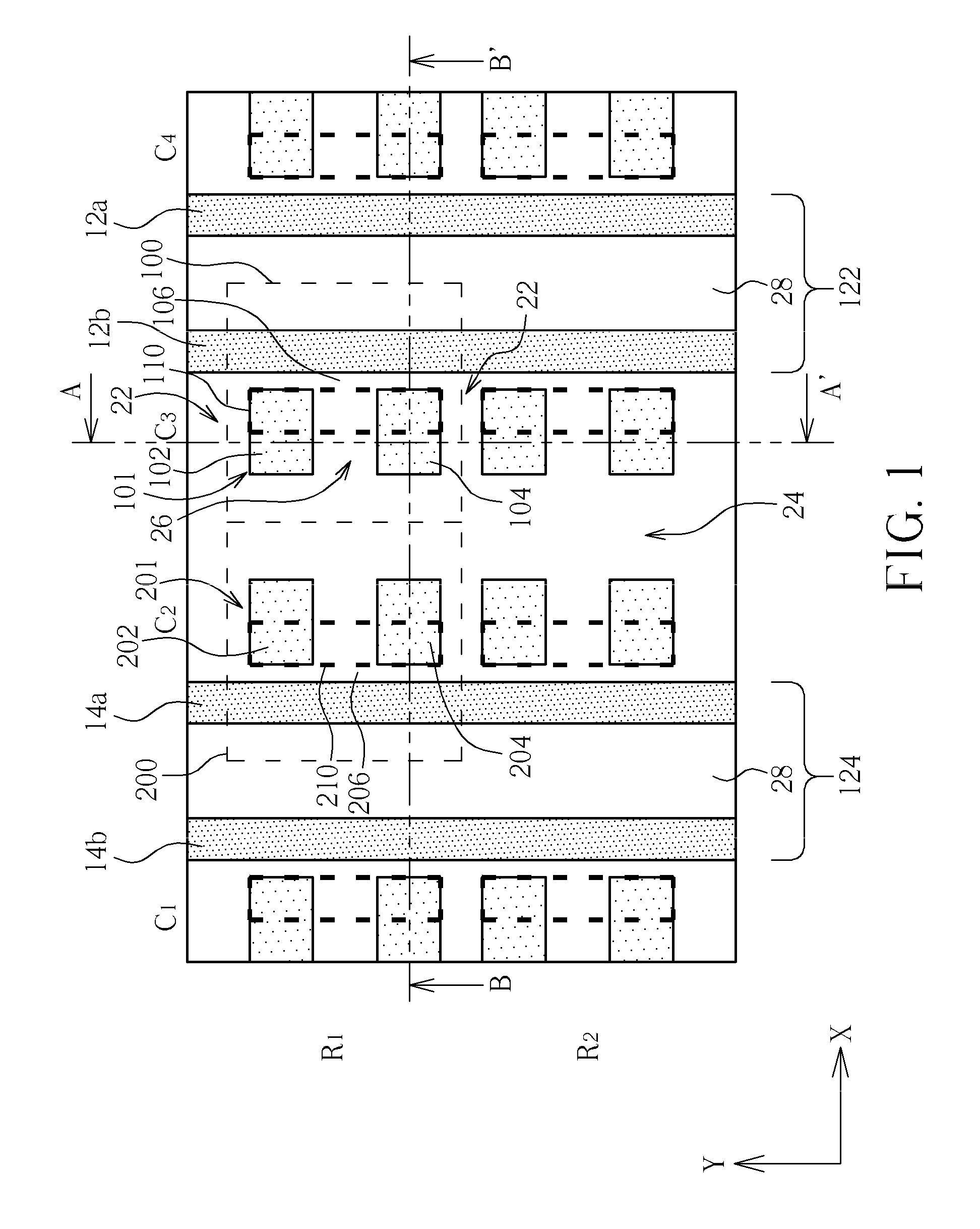
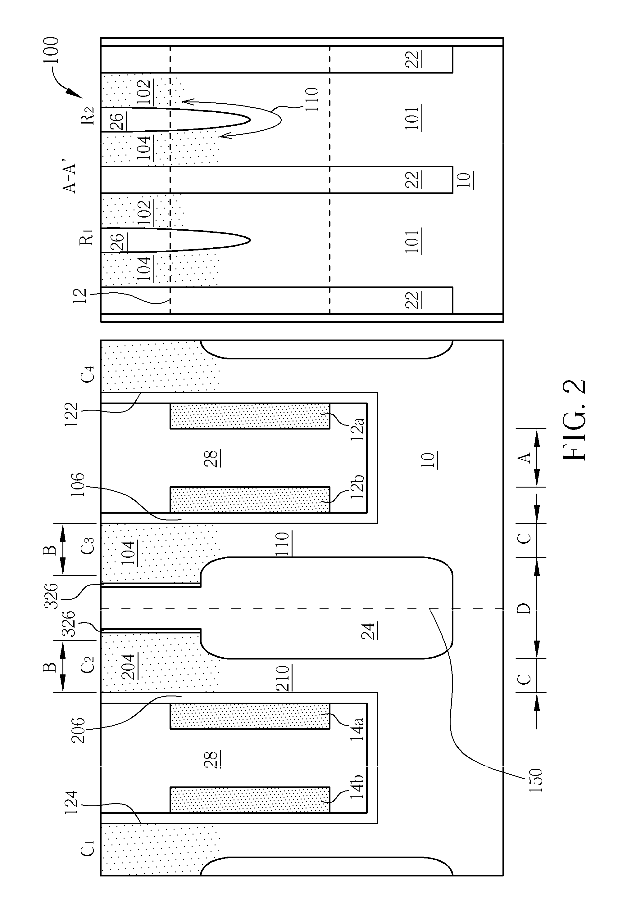
[0020]In the following description, numerous specific details are given to provide a thorough understanding of the invention. However, it will be apparent to one skilled in the art that the invention may be practiced without these specific details. In order to avoid obscuring the present invention, some well-known system configurations and process steps are not disclosed in detail.

[0021]Likewise, the drawings showing embodiments of the apparatus are semi-diagrammatic and not to scale and, particularly, some of the dimensions are for the clarity of presentation and are shown exaggerated in the figures. Also, in which multiple embodiments are disclosed and described having some features in common, for clarity and ease of illustration and description thereof, like or similar features will ordinarily be described with like reference numerals.

[0022]The term “horizontal” as used herein is defined as a plane parallel to the conventional major plane or primary surface of the semiconductor s...


PUM


Abstract

A single-gate FinFET structure includes an active fin structure having two enlarged head portions and two respective tapered neck portions that connect the enlarged head portions with an underlying ultra-thin body. Two source / drain regions are doped in the two enlarged head portions respectively. An insulation region is interposed between the two source / drain regions. A trench isolation structure is disposed at one side of the tuning fork-shaped fin structure. A single-sided sidewall gate electrode is disposed on a vertical sidewall of the active fin structure opposite to the trench isolation structure.

Description

BACKGROUND OF THE INVENTION[0001]1. Field of the Invention[0002]The present invention relates to a single-gate fin field-effect-transistor (FinFET) with an ultra-thin body (UTB).[0003]2. Description of the Prior Art[0004]As known in the art, dynamic random access memory (DRAM) is a type of random access memory that stores each bit of data in a separate capacitor within an integrated circuit. Typically, DRAM is arranged in a square array of one capacitor and transistor per cell. The transistor, which acts as switching device, comprises a gate and a silicon channel region underneath the gate. The silicon channel region is located between a pair of source / drain regions in a semiconductor substrate and the gate is configured to electrically connect the source / drain regions to one another through the silicon channel region.[0005]A vertical double-gate fin field-effect-transistor (FinFET) has been developed for the next-generation 4F2 DRAM cell (F stands for minimum lithographic feature w...

Claims


Application Information

Patent Timeline
Patent Type & Authority Applications(United States)
IPC IPC(8): H01L29/66
CPCH01L27/10826H01L29/7853H01L29/66818H01L27/10879H10B12/36H10B12/056
Inventor RENN, SHING-HWA
Owner NAN YA TECH
Why Eureka
Try Eureka