Self-aligned contact for silicon-on-insulator devices

a silicon-on-insulator and self-aligning technology, applied in the direction of semiconductor devices, electrical equipment, transistors, etc., can solve the problems of gate substantially controlling the on and off state, gate oxide thickness, gate oxide thickness, and gate oxide thickness becoming increasingly difficult to meet in conventional device structures where bulk silicon substrates are used, and significant variations in the electrical characteristics of the devi

Inactive Publication Date: 2007-02-06
TAIWAN SEMICON MFG CO LTD
View PDF11 Cites 10 Cited by
  • Summary
  • Abstract
  • Description
  • Claims
  • Application Information

AI Technical Summary

Problems solved by technology

As the gate length of the conventional bulk metal-oxide-semiconductor field-effect transistor (MOSFET) is reduced, it suffers from problems related to the inability of the gate to substantially control the on and off states of the channel.
However, for device scaling well into the sub-30 nm regime, the requirements for body doping concentration, gate oxide thickness, and source / drain (S / D) doping profiles become increasingly difficult to meet in conventional device structures where bulk silicon substrates are employed.
In addition, variations in the series resistance in the source and drain regions of the device result in significant variations in the electrical characteristics of the device.

Method used


Image

  • Self-aligned contact for silicon-on-insulator devices
  • Self-aligned contact for silicon-on-insulator devices
  • Self-aligned contact for silicon-on-insulator devices

Examples


Embodiment Construction

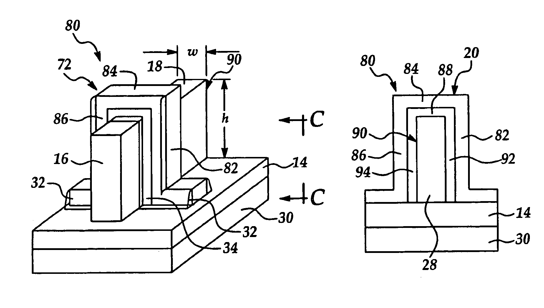
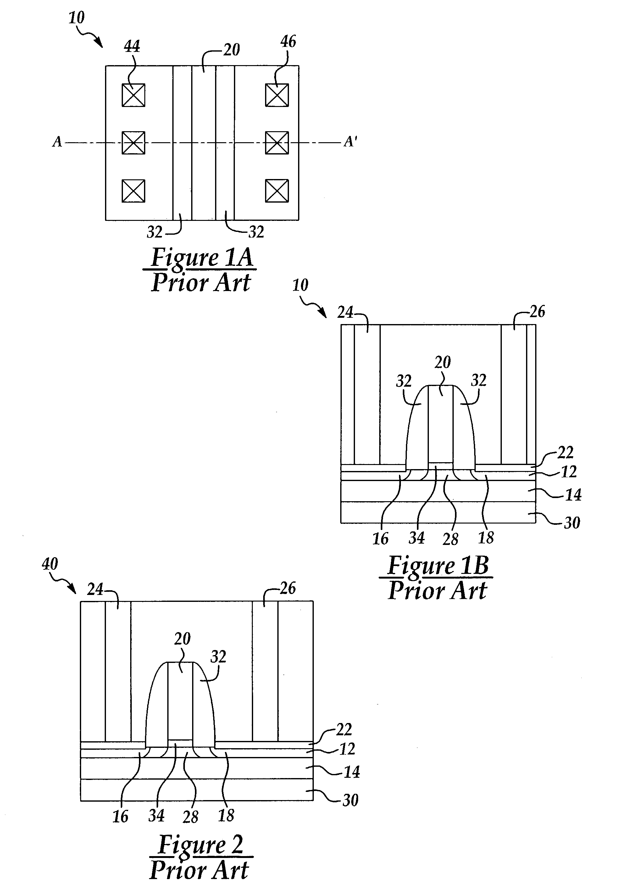
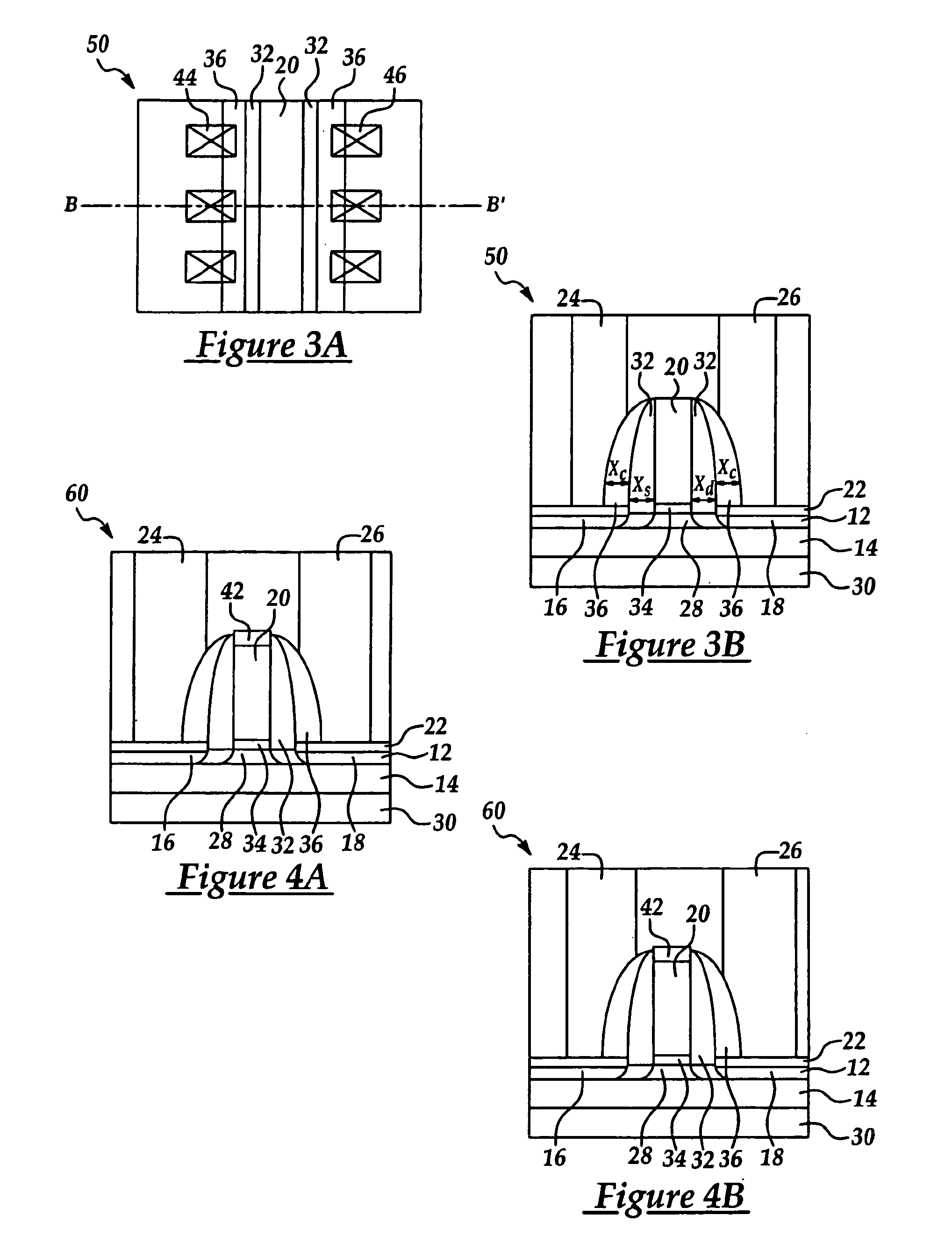
[0033]The present invention concerns the provision of self-aligned contacts to the source and drain regions in advanced semiconductor device structures such as ultra-thin body transistors, double-gate transistors such as the finFET transistor, triple-gate transistors, and omega-FET. Transistors with two or more gates, including the double-gate transistor, the triple-gate transistor, and the omega-FET are termed “multiple-gate transistors”.

[0034]In FIG. 3A, the plane view of an improved contact scheme for the UTB transistor 50 is shown. An enlarged, cross-sectional view through the dash line B–B′ of FIG. 3A is shown in FIG. 3B. The contacts 24,26 overlap a contact spacer 36, so that any slight misalignment in the source and drain contacts 24,26 will not affect the distance between the source contact 24 and the channel region 28 and the distance between the drain contact 26 and the channel region 28. The distances between the source contact 24 or the drain contact 26 and the channel r...


PUM


Abstract

A method for forming a self-aligned contact to an ultra-thin body transistor first providing an ultra-thin body transistor with source and drain regions operated by a gate stack; forming a contact spacer on the gate stack; forming a passivation layer overlying the transistor; forming a contact hole in the passivation layer exposing the contact spacer and the source / drain regions; filling the contact hole with an electrically conductive material; and establishing electrical communication with the source / drain region.

Description

FIELD OF THE INVENTION [0001]The present invention generally relates to the field of semiconductor devices and more particularly, to the manufacture of advanced metal oxide semiconductor field effect transistors (MOSFETs) with self-aligned contacts.BACKGROUND OF THE INVENTION [0002]Transistor scaling has provided continued improvement in speed performance and circuit density in ultra-large scale integrated (ULSI) chips over the past few decades. As the gate length of the conventional bulk metal-oxide-semiconductor field-effect transistor (MOSFET) is reduced, it suffers from problems related to the inability of the gate to substantially control the on and off states of the channel. Phenomena such as reduced gate control associated with transistors with short channel lengths are termed short-channel effects. Increased body doping concentration, reduced gate oxide thickness, and ultra-shallow source / drain junctions are ways to suppress short-channel effects. However, for device scaling...

Claims


Application Information

Patent Timeline
Patent Type & Authority Patents(United States)
IPC IPC(8): H01L21/336H01L29/772H01L21/60H01L29/786
CPCH01L21/76897H01L29/41791H01L29/6656H01L29/66795H01L29/785H01L29/6659H01L2029/7858H01L2924/3011
Inventor YANG, FU-LIANGYEO, YEE-CHIATSENG, HORNG-HUEIHU, CHENMING
Owner TAIWAN SEMICON MFG CO LTD
Why Eureka
Try Eureka