Clock multiplying circuit, solid-state imaging device, and phase-shift circuit

a technology of solid-state imaging and clock multiplying circuit, which is applied in the field of clock multiplying circuit, solid-state imaging device, phase-shift circuit, can solve the problems of difficulty in sufficiently dealing with the frequency change of the input clock signal, and achieve the effect of improving the output accuracy of a comparison result in a median value of a fluctuation range of a potential difference signal in the differential detection unit, stably and highly accurately generated, and improving the output accuracy of a comparison

Inactive Publication Date: 2011-12-08
SONY CORP
View PDF12 Cites 10 Cited by
  • Summary
  • Abstract
  • Description
  • Claims
  • Application Information

AI Technical Summary

Benefits of technology

[0024]Therefore, it is desirable to provide a clock multiplying circuit, a solid-state imaging device including the clock multiplying circuit, and a phase-shift circuit that can accurately obtain a clock signal with a desired duty ratio even if an operating frequency substantially fluctuates.
[0029]In the embodiments, when the double signal is generated in the operation, if the frequency of the first clock signal increases, the control current supplied to the first and second inverters is increased. Consequently, even if the frequency of the first clock signal increases, the amplitude of the potential difference signal between both the electrodes of the capacitive element can be set sufficiently large. Output accuracy of a comparison result in a median value of a fluctuation range of a potential difference signal in the differential detecting unit can be improved. Further, the differential detecting unit generates the second clock signal on the basis of a comparison result in a median value of a fluctuation range of the input potential signal. Therefore, irrespective of a change in the frequency of the first clock signal, the second clock signal can be stably and highly accurately generated.
[0030]As explained above, in the multiplying circuit according to the embodiment, even if the frequency of an input clock signal changes, a potential difference signal between both the electrodes of the capacitive element detected by the differential detecting unit can be set sufficiently large. In the embodiments, irrespective of a change in the frequency of the input clock signal, the clock signal having a phase difference of 90 degrees with respect to the positive-phase signal of the first clock signal can be stably and highly accurately generated. Therefore, in the embodiments, even if the frequency of the input clock signal changes, a double clock signal with a duty ratio of 50% can be accurately generated.

Problems solved by technology

However, when the multiplying circuit having the configuration proposed in Patent Document 2 or the like is used, there are problems explained below.
As a result, in the multiplying circuit 200 proposed in Patent Document 2 or the like, it is difficult to sufficiently deal with a frequency change of an input clock signal.

Method used


Image

  • Clock multiplying circuit, solid-state imaging device, and phase-shift circuit
  • Clock multiplying circuit, solid-state imaging device, and phase-shift circuit
  • Clock multiplying circuit, solid-state imaging device, and phase-shift circuit

Examples


Embodiment Construction

[0040]Examples of a multiplying circuit, a phase-shift circuit, and a solid-state imaging device including the multiplying circuit according to an embodiment of the present invention are explained in the following order with reference to the accompanying drawings. The present invention is not limited to the example explained below.

[0041]1. Configuration example of the multiplying circuit

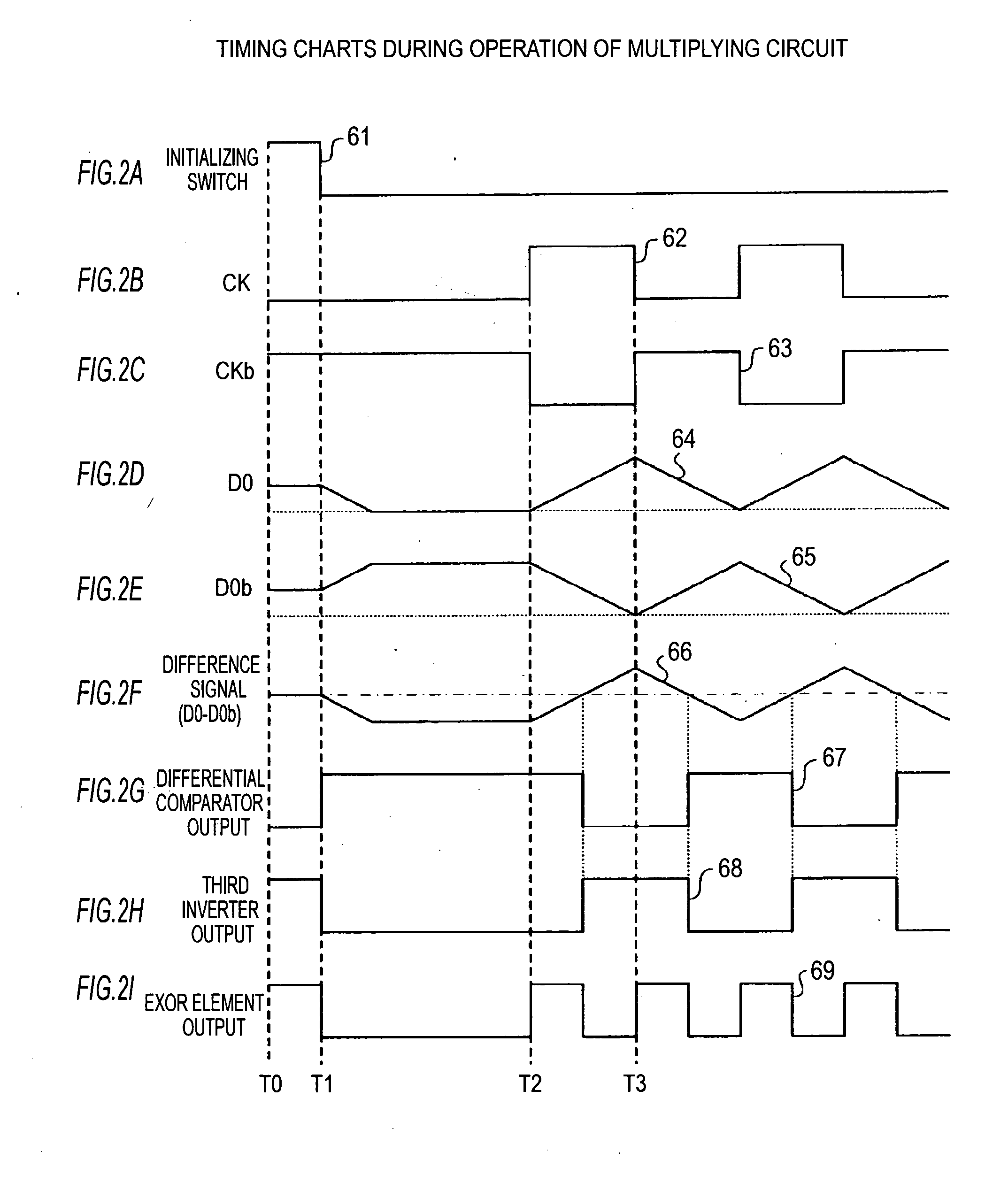
[0042]2. Operation example of the multiplying circuit

[0043]3. Configuration example of the solid-state imaging device

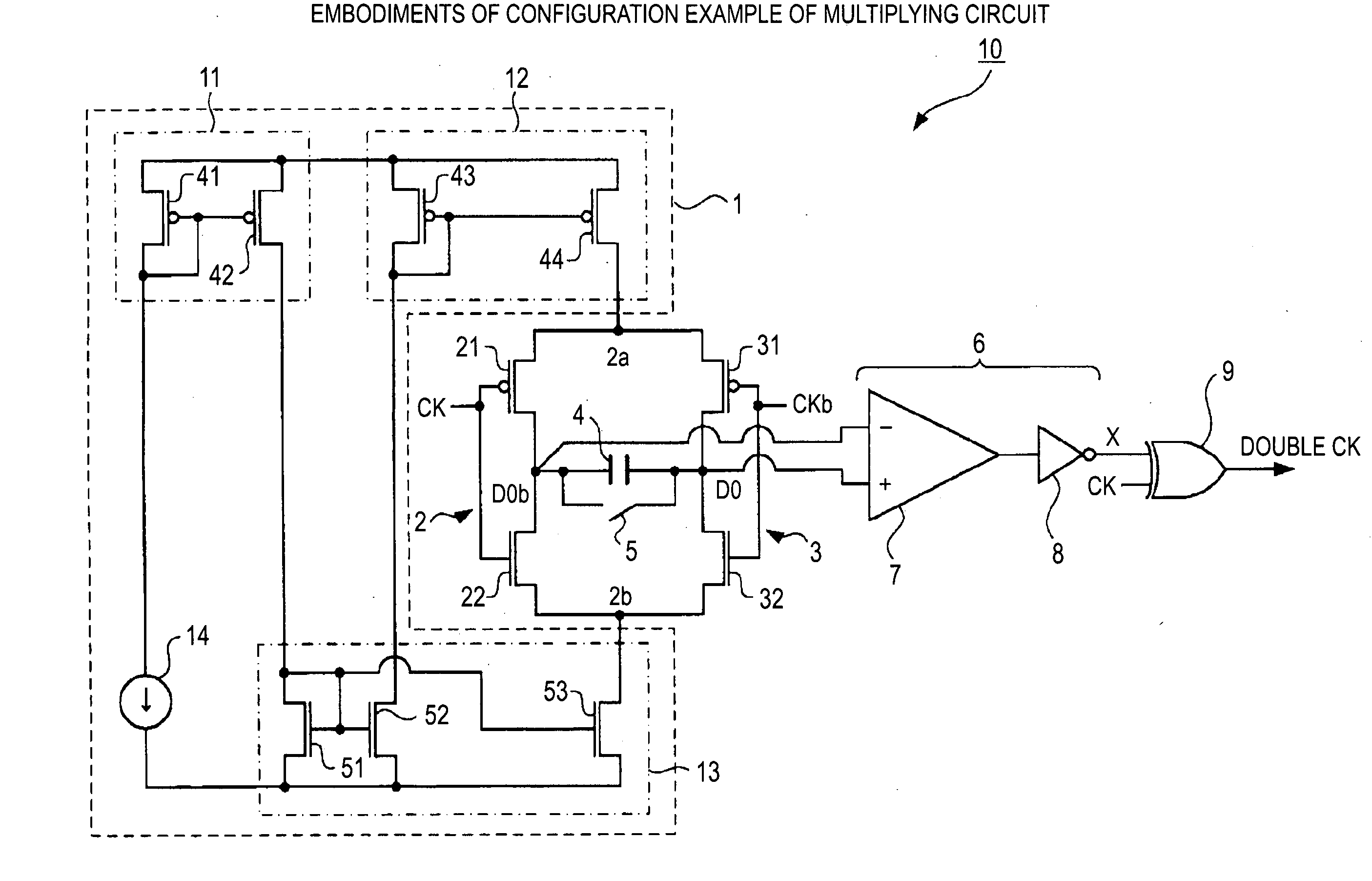
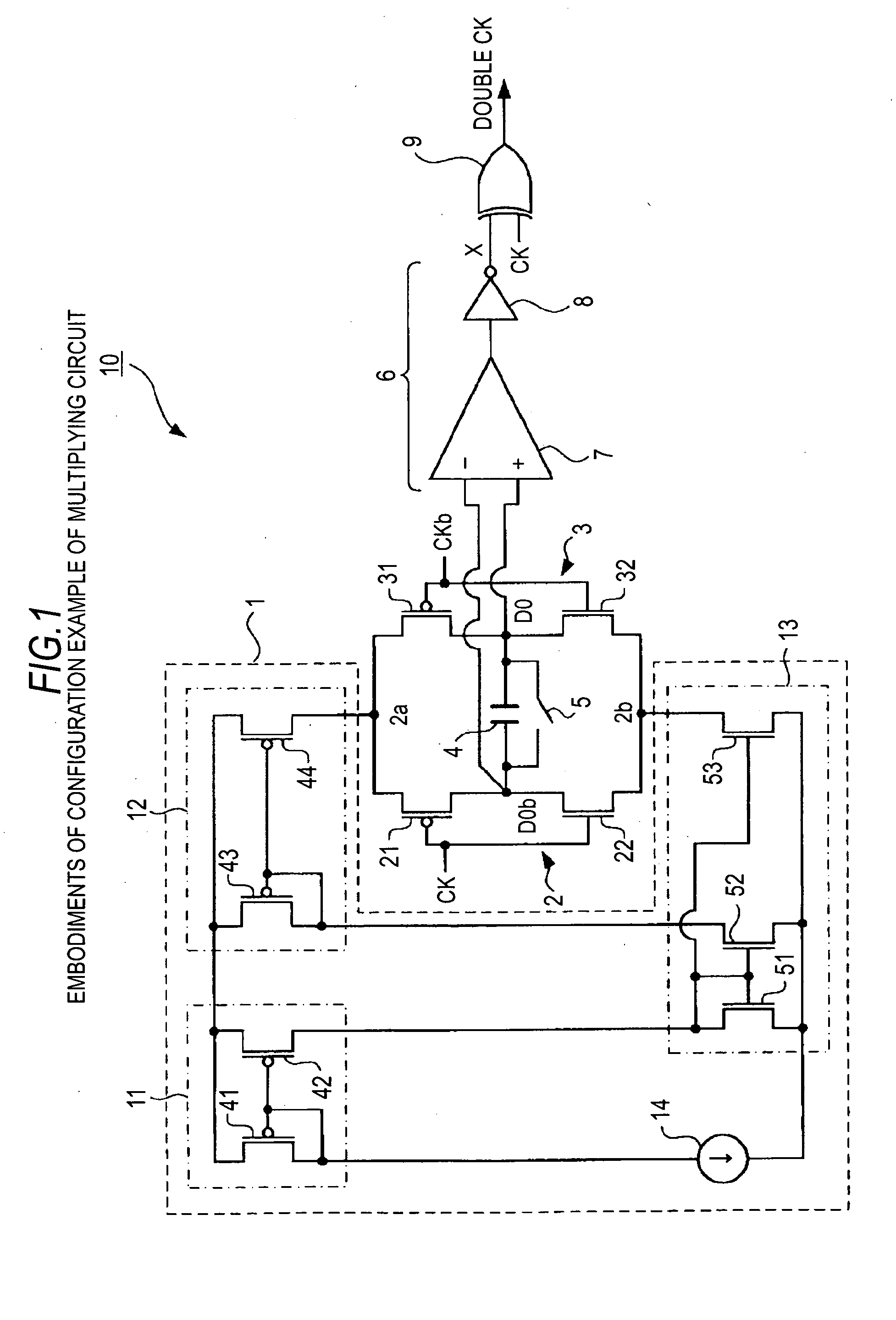
[0044]A schematic configuration of the multiplying circuit according to the embodiment of the present invention is shown in FIG. 1. A multiplying circuit 10 (a clock multiplying circuit) includes a current supplying unit 1, a first inverter 2, a second inverter 3, a capacitive element 4, an initializing switch 5 (an initializing switch element), a differential detector 6, and an EXOR (exclusive OR) element 9 (a multiplied-signal generating unit).

[0045]The current supplying unit 1 inclu...


PUM


Abstract

A clock multiplying circuit includes: first and second inverters being ON / OFF-controlled by a positive- or negative-phase signal, respectively, of a first clock signal and including current source and current sync terminals; a capacitive element provided between output ends of the inverters; a current supplying unit increasing, if a frequency of the first clock signal increases, the control current and supplying the control current to the current source terminals of the inverters and outputting, from the current sync terminals of the inverters, a control current the same current amount as that of a control current to the current source terminal; a differential detecting unit receiving input of a potential difference signal between both electrodes of the capacitive element and generating a second clock signal having a phase difference of 90 degrees; and a multiplied-signal generating unit generating a double signal of the first clock signal on the basis of the clock signals.

Description

BACKGROUND OF THE INVENTION[0001]1. Field of the Invention[0002]The present invention relates to a circuit that multiplies a clock signal by two, a solid-stage imaging device including the circuit, and a phase-shift circuit for the clock signal.[0003]2. Description of the Related Art[0004]In the past, in various electronic apparatuses, clock signals have been used to control the operations of the electronic apparatuses. Examples of the control include operation control for a 2:1 parallel-to-serial conversion circuit or the like (see, for example, JP-A-2002-9629 (Patent Document 1)).[0005]A schematic configuration of the 2:1 parallel-to-serial conversion circuit described in Patent Document 1 is shown in FIG. 4. The 2:1 parallel-to-serial conversion circuit shown in FIG. 4 is used for a circuit of a USB (Universal Serial Bus) interface or the like that converts parallel data into serial data and outputs the serial data.[0006]A 2:1 parallel-to-serial conversion circuit 100 includes tw...

Claims


Application Information

Patent Timeline
Patent Type & Authority Applications(United States)
IPC IPC(8): H04N5/335H03H11/22H03K5/00
CPCG06F7/68H03K5/00006H04N5/3765H03M9/00H03K5/1565H04N25/745
Inventor HORIMOTO, SATSUKIKAWAGUCHI, SHUNJIMATSUMOTO, SHIZUNORI
Owner SONY CORP
Why Eureka
Try Eureka