
Electronic-circuit assembling process and electronic-circuit assembling system

a technology of electronic circuits and assembling systems, applied in the field of electronic circuit assembling processes, can solve problems such as the inability to ignore the degree of functional performance variation

Active Publication Date: 2011-12-15
FUJI MASCH MFG CO LTD
View PDF6 Cites 44 Cited by
  • Summary
  • Abstract
  • Description
  • Claims
  • Application Information

AI Technical Summary

Benefits of technology

[0014]Where an electronic circuit is to be manufactured by mounting the plurality of electronic circuit components including the at least one of the different-property components, onto the circuit board; it is possible to increase a degree of freedom in operation carried out in an assembling workshop for assembling the electronic circuit, without predetermining at least one of the electrical property value and the component supply position of the at least one of the different-property components, namely, by allowing the at least one of the electrical property value and the component supply position to be determined in the assembling workshop. The increase of the degree of freedom in the operation in the assembling workshop makes it advantageously possible to perform the manufacturing of the electronic circuit in a manner satisfying limiting conditions that are likely to be required in the assembling workshop.
[0113]LED has many advantages such as high energy efficiency, long service life and low cost. However, in today's manufacturing technology, it is still difficult to manufacture LED such that the manufactured LED is provided with a highly accurate and constant brightness. The backlight or the like is required to have brightness that is uniform over an entirety of its light emitting surface. The LED is sensibly influenced by factors such as change of environment (e.g., temperature and humidity) in process of manufacture of the LED. For example, its property, particularly, its brightness exhibited upon supply of a rated current to the LED is likely to be variable depending on variation of the manufacture environment. That is the LED corresponds to a property-variable component which has an electrical property value that is variable at a plurality of levels and which could be, for example, handled as if being a property-non-variable component (i.e., electronic circuit component whose electrical property is not variable at a plurality of levels) in a case where a control is performed to merely control mounting of the component onto the circuit board. In other words, the LEDs correspond to the above-described different-property components which have respective electrical properties such that the electrical properties of at least two of the different-property components are different from each other, and which can be handled as if being components that are same as each other, in a control for controlling mounting of the components onto the circuit board. In view of this, the LEDs are sorted into a plurality of groups of respective different brightness levels, and the LEDs sorted into the same group and having the same brightness levels are mounted onto a single circuit board or onto each one of a plurality of areas within the single circuit board, so that it is considered that the brightness could be made uniform over n entirety of the light emitting surface, by controlling an electric current (that is supplied to each of the LEDs) by at least one resistor. In the electronic-circuit assembling process according to this mode (15), owing to the provision of the brightness-level-related information onto the circuit board together with the mounting of the LEDs onto the circuit board, it is possible to mount, onto the circuit board, the at least one resistor suitable for the brightness of the LEDs that have been actually mounted onto the circuit board. For example, even in a case where the LED actually mounted on the circuit board has a brightness level that mismatches with a predetermined brightness level for some reason, the property-related information that is provided after the mounting of the LEDs onto the circuit board makes it possible to reliably mount, onto the circuit board, the at least one resistor which is suitable for the brightness of the LEDs having been actually mounted onto the circuit board, namely, which is to be associated with the actually mounted LEDs.

Problems solved by technology

There is a case where such a variation of the degree of functional performance is not ignorable.

Method used


Image

  • Electronic-circuit assembling process and electronic-circuit assembling system
  • Electronic-circuit assembling process and electronic-circuit assembling system
  • Electronic-circuit assembling process and electronic-circuit assembling system

Examples


Embodiment Construction

[0030]There will be described various modes of the invention deemed to contain claimable features for which protection is sought. Hereinafter, the invention deemed to contain the claimable features will be referred to as “claimable invention” where appropriate. The claimable invention includes at least “the present invention” or “the invention of the present application” which is an invention described in claims, and could include also specific concept of the invention of the present application, generic concept of the invention of the present application and other concept of the invention of the present application. Each of these modes of the invention is numbered like the appended claims and depends from the other mode or modes, where appropriate, for easier understanding of the technical features disclosed in the present specification. It is to be understood that the claimable invention is not limited to the technical features or any combinations thereof which will be described i...


PUM

PropertyMeasurementUnit
electrical propertiesaaaaaaaaaa
electrical propertyaaaaaaaaaa
electrical characteristicsaaaaaaaaaa

Abstract

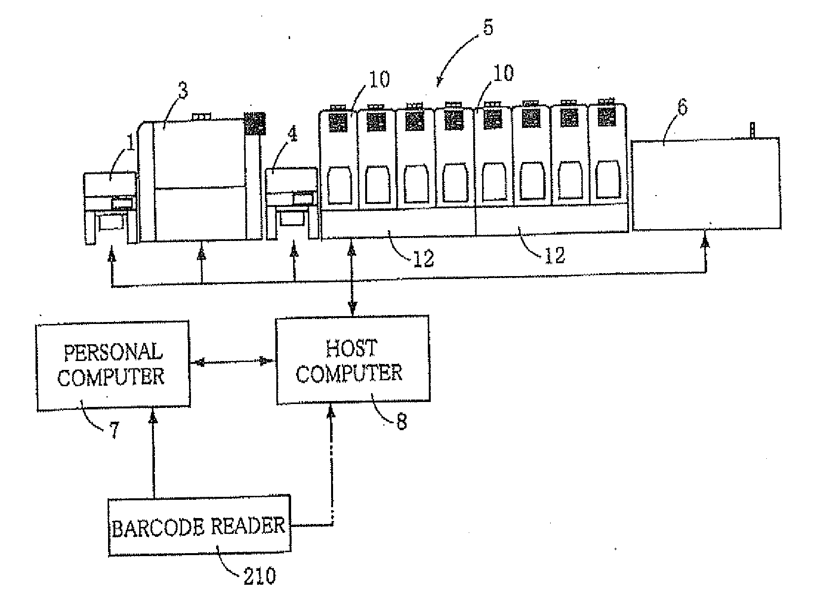
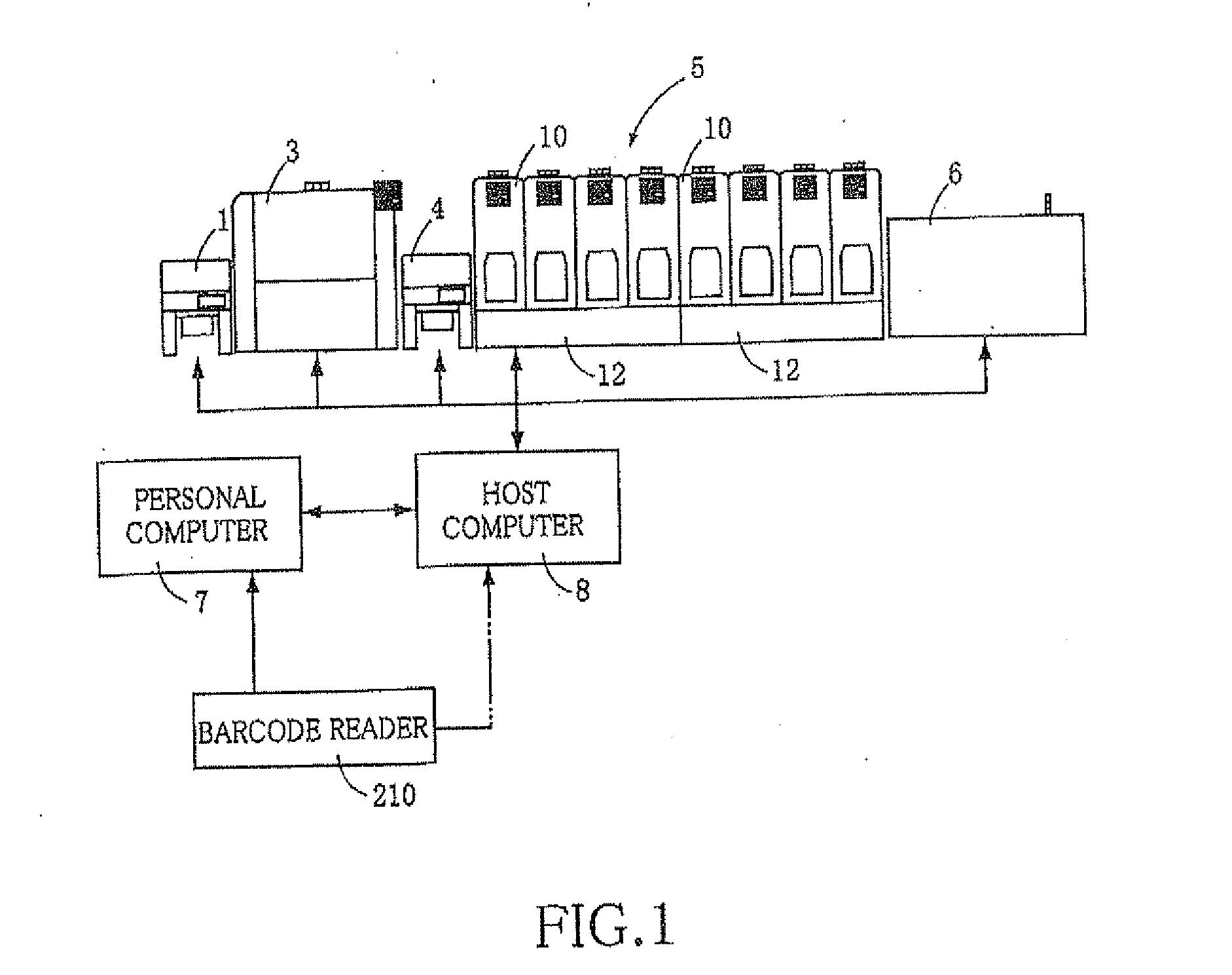
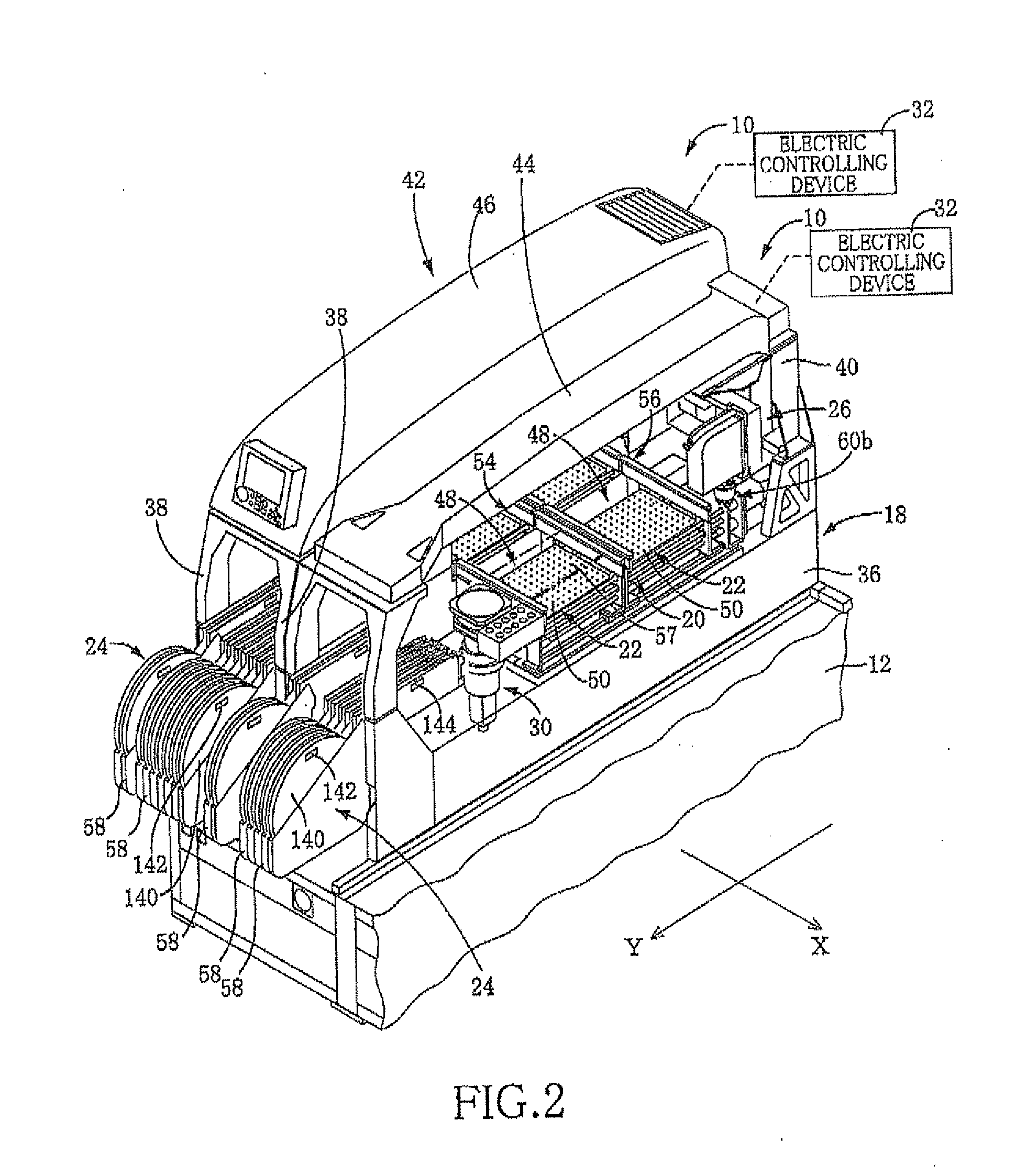
An electronic-circuit assembling process to be carried out in an electronic-circuit assembling system, for assembling an electronic circuit, by mounting electronic circuit components supplied from a component supplier, onto a circuit board, wherein the electronic circuit components includes at least one of different-property components having respective different electrical properties. The process includes: (a) a different-property-component-related information obtaining step of obtaining a different-property-component-related information including (a-i) a property-related information that enables recognition of the electrical property of the different-property component supplied from the component supplier and (a-ii) a different-property-component supply position that is a position of the component supplier supplying the different-property component, such that the different-property-component-related information is obtained by detecting the property-related information and / or the different-property-component supply position; (b) a mounting step of mounting, based on information related to the different-property-component supply position, the electronic circuit components including the different-property component, onto the circuit board; and (c) a property-related information providing step of providing the circuit board with the property-related information of the different-property component mounted on the circuit board.

Description

CROSS REFERENCE TO RELATED APPLICATION[0001]This application claims priority from Japanese Patent Application No. 2010-138232 filed on Jun. 10, 2010, the disclosure of which is herein incorporated by reference in its entirety.BACKGROUND OF THE INVENTION[0002]1. Field of the Invention[0003]The present invention relates to a process and a system for assembling an electronic circuit by mounting electronic circuit components onto a circuit board.[0004]2. Discussion of Related Art[0005]As disclosed in JP2003-283199A, there is known a technique for providing a circuit board with information representing electrical characteristics or properties of electronic circuit components that are mounted on the circuit board. This publication of the Japanese Patent Application discloses an electronic-circuit assembling system including two electronic-circuit-component mounters each of which is configured to mount a corresponding one of two kinds of electronic circuit components, onto the circuit boar...

Claims


Application Information

Patent Timeline
Patent Type & Authority Applications(United States)
IPC IPC(8): H05K3/00
CPCH05K13/0452Y10T29/49124H05K13/08H05K13/084H05K13/085
Inventor KATO, DAISUKEHANEDA, HIROYUKI
Owner FUJI MASCH MFG CO LTD
Learn More