Fingerprint sensing circuit

Active Publication Date: 2011-12-15
SYNAPTICS INC
View PDF5 Cites 83 Cited by
  • Summary
  • Abstract
  • Description
  • Claims
  • Application Information

AI Technical Summary

Benefits of technology

[0004]Some embodiments of the disclosure provide a fingerprint sensing circuit package including at least one substrate with a first top side and a second bottom side. The first top side can be a sensing side for a user's fingerprint to be swiped over. The second side can include fingerprint sensing circuitry such a

Problems solved by technology

The barrier material often determines the cost

Method used


Image

  • Fingerprint sensing circuit
  • Fingerprint sensing circuit
  • Fingerprint sensing circuit

Examples


Embodiment Construction

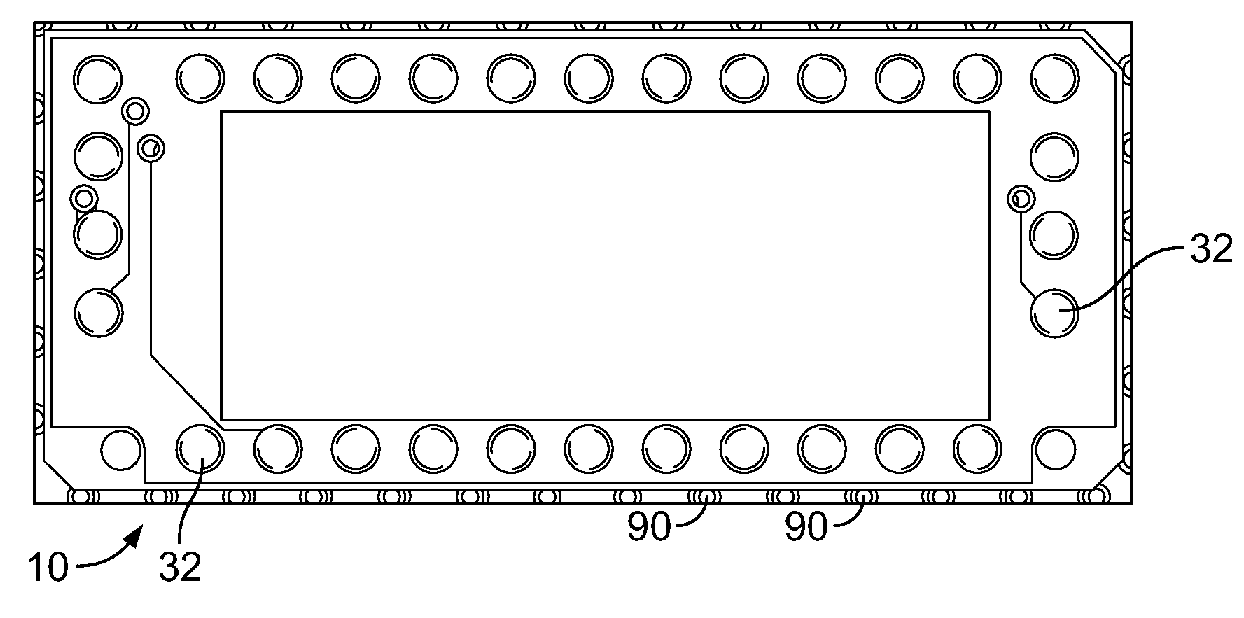
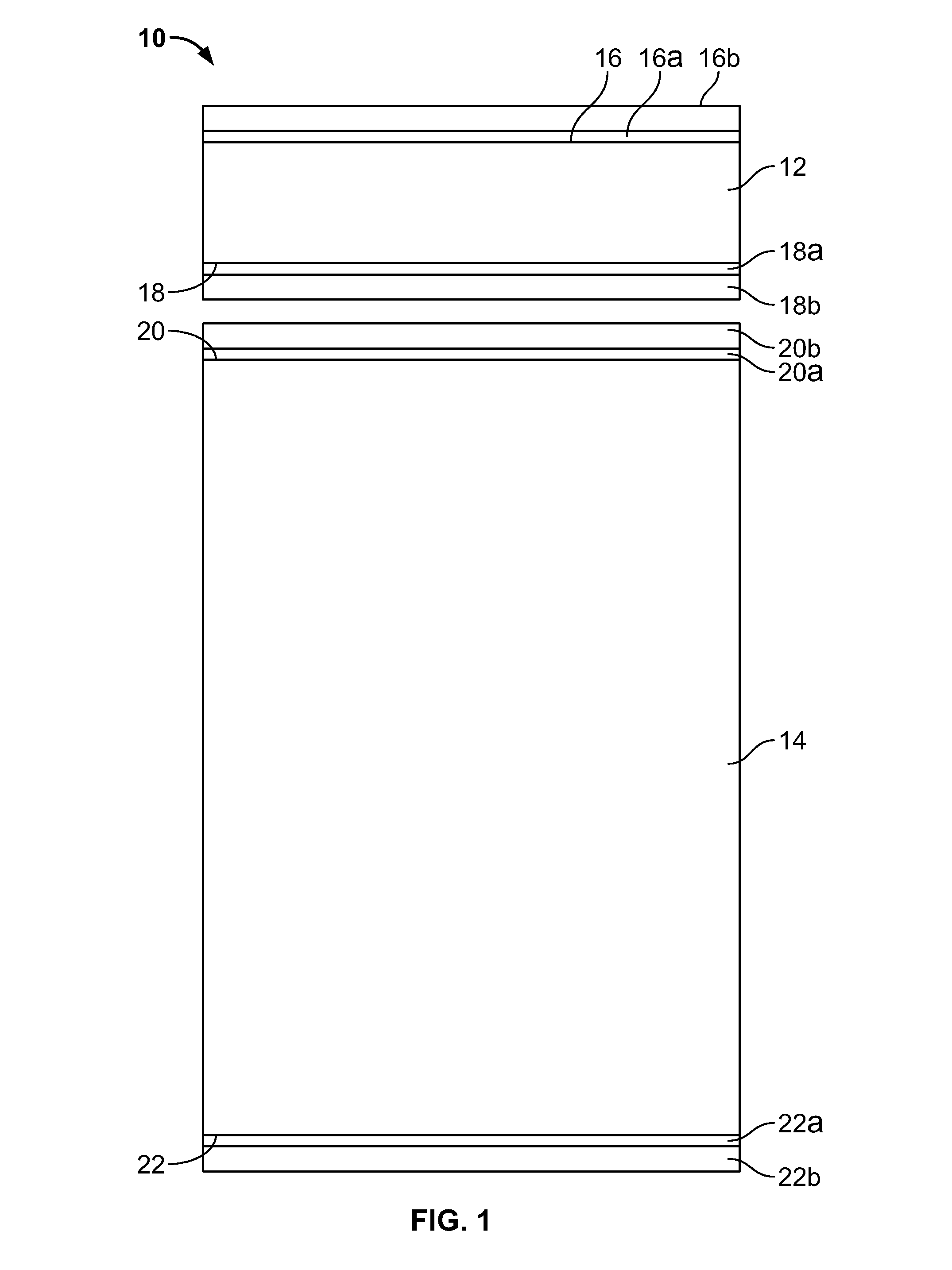
[0024]FIG. 1 shows a side view of a conventional fingerprint sensing circuit package 10 which can be used in some embodiments of the disclosed subject matter, for use in housing fingerprint image sensing and image reconstruction circuitry as is discussed in more detail in, e.g., U.S. Pat. No. 7,751,601, entitled, FINGER SENSING ASSEMBLIES AND METHODS OF MAKING, issued on Jul. 6, 2010, U.S. Pat. No. 7,460,697, entitled ELECTRONIC FINGERPRINT SENSOR WITH DIFFERENTIAL NOISE CANCELLATION, issued on Dec. 2, 2008, U.S. Pat. No. 7,146,024, entitled SWIPED APERTURE CAPACITIVE FINGERPRINT SENSING SYSTEM AND METHODS, issued on Dec. 5, 2006 and U.S. Pat. No. 7,099,496, entitled SWIPED APERTURE CAPACITIVE FINGERPRINT SENSING SYSTEM AND METHODS, each owned at least in part by the assignee of the present application, the disclosures of each of which are hereby incorporated by reference in their entirety.

[0025]The two substrates, an upper substrate 12 and a lower substrate 14, can define four main...


PUM


Abstract

Fingerprint sensing circuit packages and methods of making such packages may comprise a first substrate having a top side and a bottom side; the top side comprising a fingerprint image sensing side over which a user's fingerprint is swiped; the bottom side comprising a metal layer forming a fingerprint sensing circuit image sensor structure; and a sensor control circuit housed in a sensor control circuit package mounted on the metal layer. The sensor control circuit may comprise an integrated circuit die contained within the sensor control circuit package. The fingerprint sensing circuit package may also have a second substrate attached to the bottom side of the first substrate having a second substrate bottom side on which is placed connector members connecting the fingerprint sensing circuit package to a device using a fingerprint image generated from the fingerprint sensing circuitry contained in the fingerprint sensing circuitry package.

Description

CROSS-REFERENCE[0001]This application claims the benefit of U.S. Provisional Application No. 61 / 306,392, filed Feb. 19, 2010, entitled “Fingerprint Sensing Circuit” which application is incorporated herein by reference.BACKGROUND OF THE INVENTION[0002]Fingerprint sensor circuitry must be protected from physical, mechanical, and electrical damage by barrier materials. The barrier material often determines the cost, size, and overall reliability of the product. All sensor types, including, but not restricted to swipe, static, silicon touch, capacitive, or sensor separated from silicon, require some form of protection over the imaging circuitry which is used to acquire the finger print image.SUMMARY OF THE INVENTION[0003]Aspects of the disclosure provide for fingerprint sensing circuit packages, methods of use and methods of manufacture.[0004]Some embodiments of the disclosure provide a fingerprint sensing circuit package including at least one substrate with a first top side and a sec...

Claims


Application Information

Patent Timeline
IPC IPC(8): H01L27/146
CPCH01L27/14678G06K9/00053G06V40/1329
Inventor ERHART, RICHARD ALEXNELSON, RICHARD BRIANTHOMPSON, ERIKPEREZSELSKY, ARMANDO LEON
Owner SYNAPTICS INC
Why Eureka
Try Eureka