Package structure for edge-emitting laser

Active Publication Date: 2020-05-28
LITE ON ELECTRONICS (GUANGZHOU) LTD +1
View PDF0 Cites 0 Cited by
  • Summary
  • Abstract
  • Description
  • Claims
  • Application Information

AI Technical Summary

Benefits of technology

This patent is about a package structure for an edge-emitting laser that uses two reflective members to change the path of the laser so that it is shorter and the light output is in the middle of the package. This makes it easier to use in portable electronic devices.

Problems solved by technology

A conventional laser diode is mounted on a substrate in a form of a lead-type package structure, wherein a perpendicular distance (greater than 9 mm) is present between a mounting surface of the substrate and a collimating lens, so that the overall height of the package structure is increased, the volume of the package structure is also relatively increased, and the drawback of occupying too much space is present.

Method used


Image

  • Package structure for edge-emitting laser
  • Package structure for edge-emitting laser
  • Package structure for edge-emitting laser

Examples


Embodiment Construction

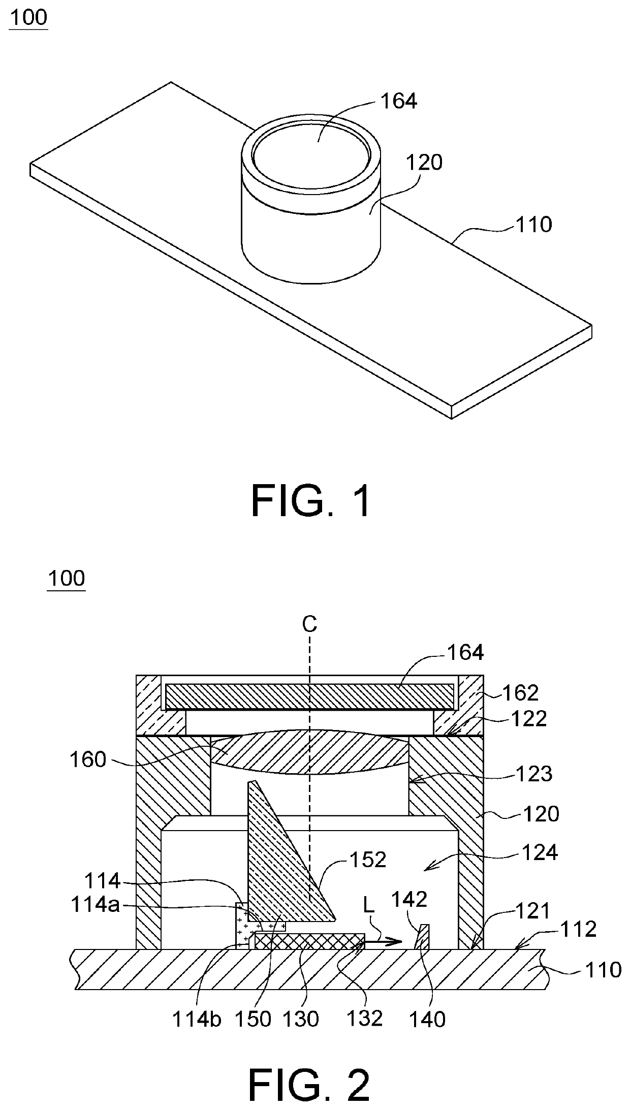
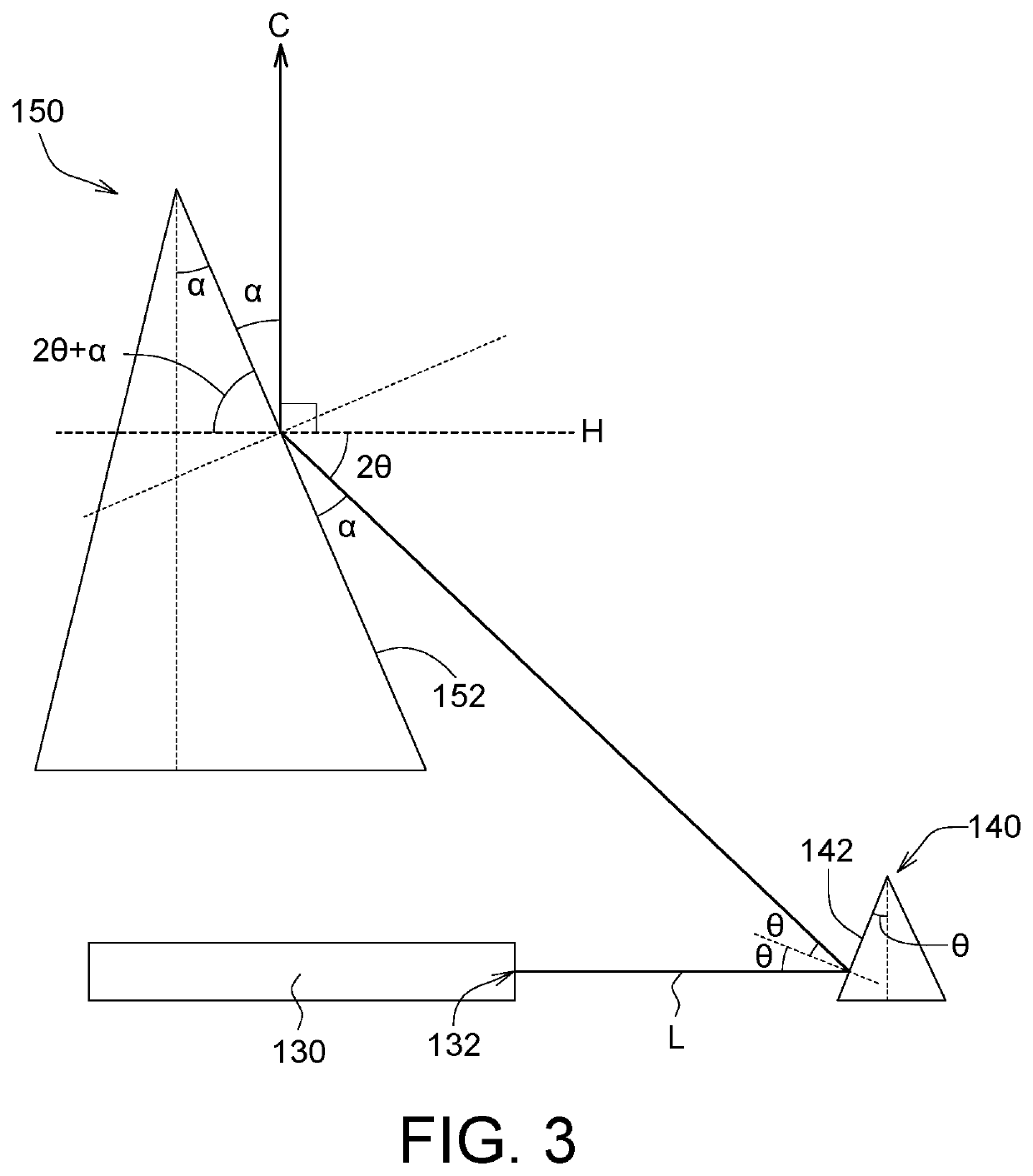
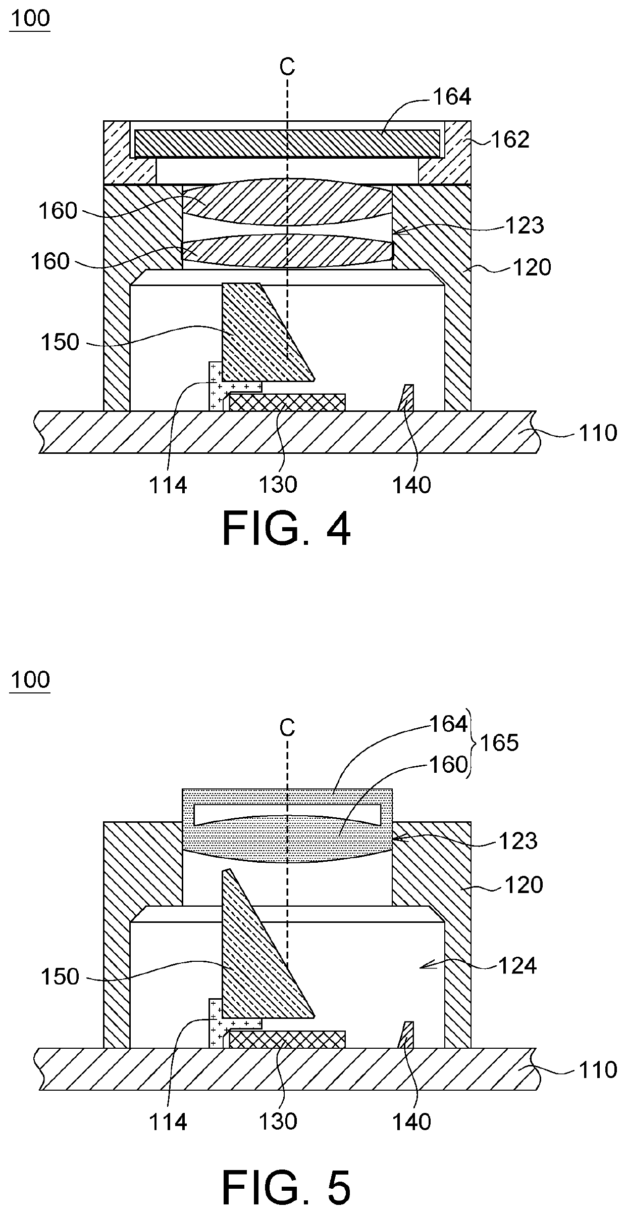
[0014]The embodiments will be described in detail herein below, and are only illustrative without limiting the scope of the invention. In the following illustration, the same / similar symbols represent the same / similar elements.

[0015]Directional terms, such as above, under, left, right, front, back and the like mentioned in the following examples, only refer to the directions based on the drawings. Therefore, the directional terms are used to describe but not to limit the invention.

[0016]According to an embodiment of the invention, a package structure for an edge-emitting laser (EEL) is provided. The edge-emitting laser is a semiconductor component, such as a gallium arsenide chip, which generates resonance by photon reflection back and forth in a resonance cavity, and makes the high energy coherent light beam emit from the light-emitting surface on the lateral side of the chip, so that the laser beam is generated and is named as the “edge-emitting laser”. This laser power is high, a...


PUM


Abstract

A package structure includes a carrier, a housing, an edge-emitting laser, first and second reflective members and a diffractive optical element. The housing disposed on a mounting surface of the carrier has a receiving space and a top surface, which has an opening and a center line perpendicular to the top surface and the mounting surface. The edge-emitting laser disposed in the receiving space and on the mounting surface has a light-emitting surface emitting a laser beam. The first reflective member is disposed in the receiving space and spaced apart from the light-emitting surface. The second reflective member is disposed in the receiving space and located on the center line above the edge-emitting laser. The diffractive optical element is disposed on the top surface. The laser beam reflected by the first and second reflective members passes through the diffractive optical element to emit out of the housing.

Description

[0001]This application claims the benefit of People's Republic of China application Serial No. 201811396691.6, filed Nov. 22, 2018, the subject matter of which is incorporated herein by reference.BACKGROUND OF THE INVENTIONField of the Invention[0002]The invention relates to a package structure, and more particularly to a package structure for an edge-emitting laser.Description of the Related Art[0003]A conventional laser diode is mounted on a substrate in a form of a lead-type package structure, wherein a perpendicular distance (greater than 9 mm) is present between a mounting surface of the substrate and a collimating lens, so that the overall height of the package structure is increased, the volume of the package structure is also relatively increased, and the drawback of occupying too much space is present.[0004]Thus, how to decrease the overall height of the package structure is a subject to be overcome in the industry.SUMMARY OF THE INVENTION[0005]The invention is directed to ...

Claims


Application Information

Patent Timeline
IPC IPC(8): H01S5/022
CPCH01S5/02292H01S5/02296H01S5/02288H01S5/0206H01S5/022H01S5/0225H01S5/02208H01S5/02253H01S5/02255H01S5/02257H01S5/02325H01S5/0071
Inventor SHIH, MING-HUANGLUO, WANG-JIE
Owner LITE ON ELECTRONICS (GUANGZHOU) LTD
Why Eureka
Try Eureka