

Meth0d and system for connecting a plurality of printed circuit boards to at least one frame or carrier element and printed circuit board and frame or carrier element
- Summary
- Abstract
- Description
- Claims
- Application Information
AI Technical Summary
Benefits of technology
Problems solved by technology
Method used
Image

Examples
Embodiment Construction
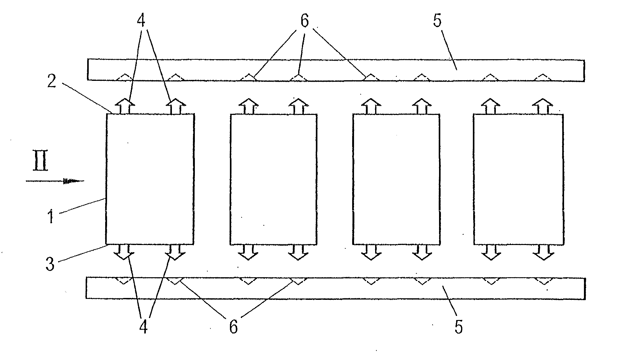
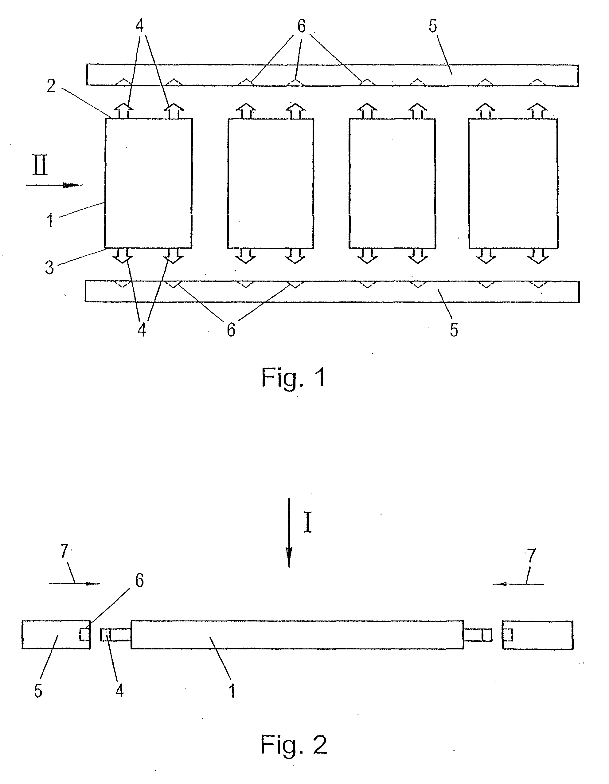
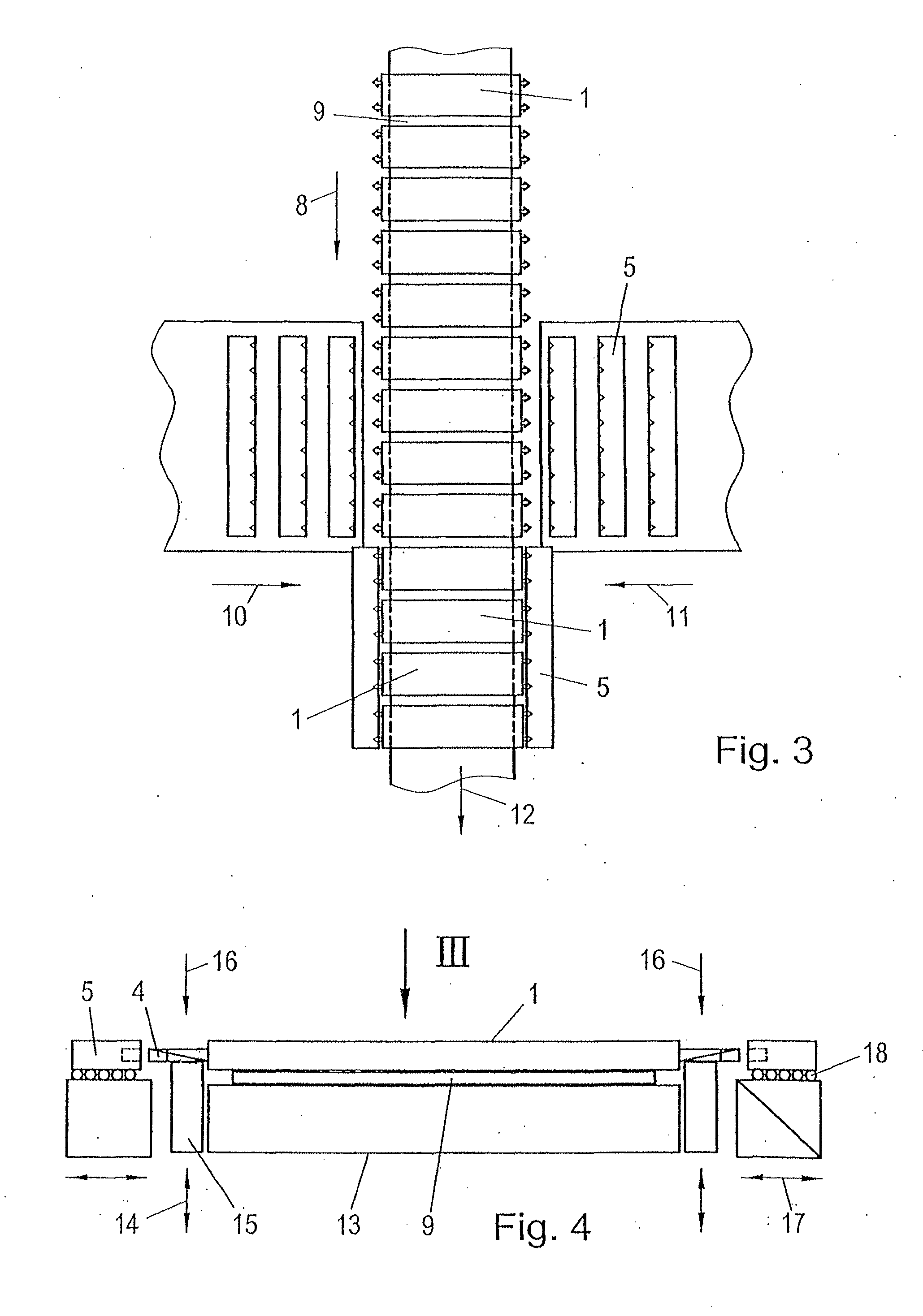
[0052]FIG. 1 schematically depicts a plurality of printed circuit boards 1, for instance, produced in the form of multilayer circuit boards in preceding method steps known per se, the printed circuit boards 1 in the embodiment illustrated in FIG. 1 being each designed to have two coupling elements 4 on oppositely located side edges 2 and 3.
[0053]In the configuration according to FIG. 1, the coupling elements 4 are each formed with a tapering cross section and, in particular, a triangular cross section in top view.
[0054]In addition, it is provided according to FIG. 1 that a frame or carrier element 5 is each provided facing the respective edges 2 and 3 of the printed circuit boards 1, which frame or carrier element is designed to have coupling elements in the form of cavities or depressions 6 corresponding to, or complementing, the coupling elements 4 of the printed circuit boards 1.
[0055]To connect or couple the printed circuit boards 1 to the frame or carrier elements 5, the frame ...
PUM
 Abstract
Description
Claims
Application Information