Bistable CML Circuit
a technology of latching and storage elements, applied in the field of latching storage elements, can solve the problems of adversely affecting the power supply voltage decrease, in each branch, of three transistors in series,
- Summary
- Abstract
- Description
- Claims
- Application Information
AI Technical Summary
Benefits of technology
Problems solved by technology
Method used
Image
Examples
Embodiment Construction
[0020]For clarity, the same elements have been designated with the same reference numerals in the different drawings.
[0021]The present invention will be described in relation with transistors in CMOS technology. The present invention can however be applied to any other transistor technology or to a combination of different technologies.
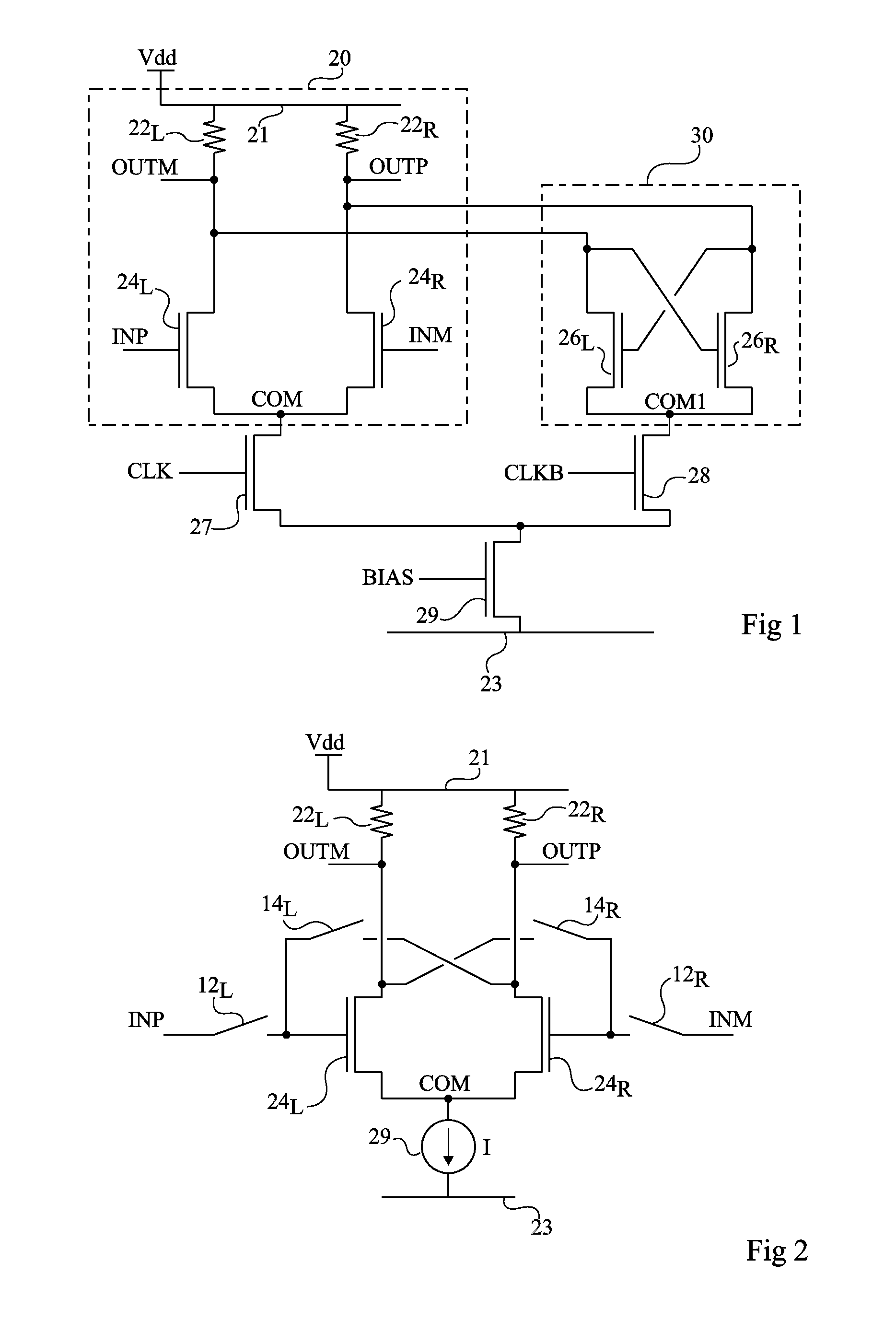
[0022]FIG. 1 shows the diagram of a latch such as described in U.S. Pat. No. 7,336,114, the relevant teaching of which is incorporated herein by reference. This latch comprises two sub-assemblies: an amplification stage 20 and a storage stage or bistable (latch) 30.
[0023]Amplification stage 20 comprises, in parallel between a terminal 21 of application of a power supply voltage Vdd (the high logic level) and a node COM, two branches, each comprising two series-assembled components: a charge resistor 22 (22L, 22R) and a transistor 24 (24L, 24R) of an input stage. Output terminals OUTP and OUTM are defined by the junction points of the series assemblies...
PUM
 Abstract
Description
Claims
Application Information


