Unlock instant, AI-driven research and patent intelligence for your innovation.

Light-Emitting Diode Packaging Structure and Substrate Therefor

a technology of led packaging and diodes, which is applied in the direction of basic electric elements, electrical apparatus, and semiconductor devices, can solve the problems of high molding cost, lower final product yield, and long molding time, and achieve the effects of improving light emission performance of the led packaging structure of the present invention, simple process and economic equipment, and good thermal conductivity

Inactive Publication Date: 2012-01-05
VIKING TECH L C
View PDF2 Cites 0 Cited by
  • Summary
  • Abstract
  • Description
  • Claims
  • Application Information

AI Technical Summary

Benefits of technology

[0007]In light of the drawbacks of the aforementioned prior art, the present invention provides an LED packaging structure that can be manufactured at a lower cost, with a higher yield, and that can have an improved light emission performance.
[0011]In the above LED packaging structure, the sidewall of the concave portion is oblique or progressively enlarged upward from the bottom. In an embodiment, the bottom of the concave portion has a die bonding area for allowing the LED die to be mounted therein and the electrically conductive pads to be formed outside the die bonding area. In another embodiment, the die bonding area on the bottom of the concave portion can be selectively electrically connected with the electrically conductive pads in order to perform a flip chip packaging of a flip-chip LED. During the flip chip packaging process, the LED chip will be turned over for electrical connecting the LED chip with the substrate, so as to decrease the signal transmitting distance between the LED chip and the substrate. It is thus suitable for the packaging of a high-speed device. In addition, the size of the final products can be reduced.
[0015]Consequently, in the LED packaging structure of the present invention, the metal substrate having good thermal conductivity is used as a carrier. The anode film can be an insulating layer between the LED die and the metal substrate. The electrically conductive pads and the conductive columns are together formed into an electrical connecting path. Thus, the metal substrate may provide not only thermal conductivity, but also electrical insulation. Moreover, the metal substrate has the concave portion thereon, such that the LED packaging process can be accomplished by applying a dispensing method which is simple in process and economic in equipment. The LED die performs an optical function through the concave portion such that the influence of the material of the formed encapsulant in the prior art can be resolved. The light emission performance of the LED packaging structure of the present invention can be improved.

Problems solved by technology

However, since the encapsulant 12 needs to be adhered to the substrate 10 and encapsulate the LED 11, a special mold or plastic frame is required to be used to form the desired encapsulant 12 by using an expensive press molding machine or injection molding machine.
Accordingly, this results in longer molding time and higher molding cost.
Further, LED 11 is vulnerable during the molding process for forming the encapsulant 12, thus making the yield of the final products lower than desired.

Method used


Image

  • Light-Emitting Diode Packaging Structure and Substrate Therefor
  • Light-Emitting Diode Packaging Structure and Substrate Therefor

Examples


Embodiment Construction

[0018]The following specific embodiment is provided to illustrate the present invention. Others skilled in the art can readily gain an insight into other advantages and features of the present invention based on the contents disclosed in this specification. The present invention can also be performed or applied in accordance with other different embodiments. Various modifications and changes based on different viewpoints and applications yet still within the scope of the present invention can be made in the details of the specification.

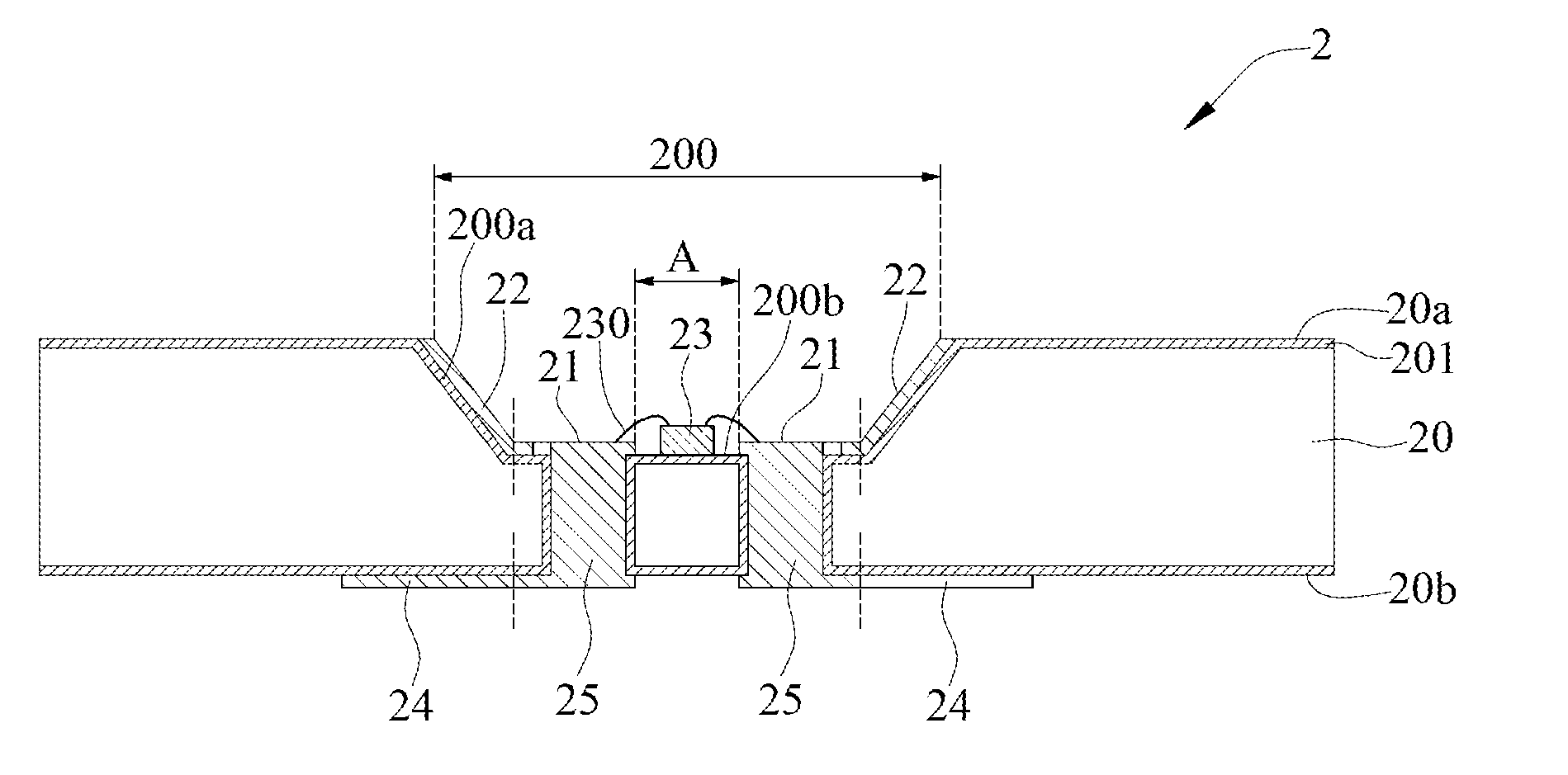
[0019]Referring to FIG. 2, an LED packaging structure 2 according to the present invention is illustrated. The LED packaging structure 2 has a metal substrate 20 having a first surface 20a and a second surface 20b opposite to the first surface 20a, a plurality of electrically conductive pads 21 and an LED die 23. The first surface 20a of the metal substrate 20 is formed with a concave portion 200 having a sidewall 200a and a bottom 200b. And, an anode...


PUM


Abstract

A light-emitting diode (LED) packaging structure and a substrate for the packaging structure are provided. The light-emitting diode packaging structure includes a metal substrate having a first surface and a second surface opposite to the first surface, and the first surface has a concave portion with a sidewall and a bottom, allowing an anode film to be formed on the metal substrate; a plurality of electrically conductive pads formed on the bottom of the concave portion; an optical treatment layer formed on the sidewall of the concave portion; and an LED die mounted on the bottom of the concave portion and electrically connected to the electrically conductive pads. Desired electrical insulating property between any two adjacent electrically conductive pads can be obtained by the anode film formed on the metal substrate, while a good thermal conductivity of the metal substrate is maintained.

Description

FIELD OF THE INVENTION[0001]The present invention relates to light-emitting structures, and more particularly to a light-emitting diode packaging structure.BACKGROUND OF THE INVENTION[0002]Light emitting diode (LED) is subject to a kind of semiconductor devices. With the rapid development of the LED technology and the increasing maturity of the technologies of the related peripheral integrated circuit control elements and heat dissipating, LED applications become more diversified. Early development for applications of LED included low-power indicator lamps and light source for mobile phone keypads. Nowadays, LEDs are applied to the LED backlight, general household lighting, and even large-scale lighting products such as electronic billboards which are lower in utility consumption, longer in lifetime and higher in color rendering index.[0003]Referring to FIG. 1, a conventional LED packaging structure 1 is illustrated for instance, which has a substrate 10 for carrying an LED 11 and a...

Claims


Application Information

Patent Timeline
IPC IPC(8): H01L33/48
CPCH01L33/486H01L33/60H01L33/62H01L33/642H01L2224/48091H01L2933/005H01L2924/00012H01L2924/00014
Inventor WEI, SHIH-LONGHSIAO, SHEN-LISHAO, CHIEN-MINHO, CHIEN-HUNG
Owner VIKING TECH L C