Semiconductor module and method of manufacturing the same

a technology of semiconductor chips and manufacturing methods, applied in the direction of semiconductor/solid-state device details, semiconductor devices, electrical apparatus, etc., can solve the problems of complex manufacturing process, uniform mounting directions of semiconductor chips, and complicated assembling process, so as to reduce the number of hanging leads

Active Publication Date: 2012-01-05
DENSO CORP
View PDF2 Cites 50 Cited by
  • Summary
  • Abstract
  • Description
  • Claims
  • Application Information

AI Technical Summary

Benefits of technology

[0036]In such a manufacturing method, during the molding, the connecting part can serve as the hanging lead while connecting the second heat sink and the third heat sink. Therefore, the number of hanging leads can be reduced.

Problems solved by technology

In such a semiconductor module, however, directions of mounting the semiconductor chips are not uniform.
Therefore, an assembling process is complicated.
Moreover, the manufacturing process is complicated.
Thus, it is difficult to reduce the size of the semiconductor module.
Accordingly, it is difficult to reduce the size of the semiconductor module J10.

Method used


Image

  • Semiconductor module and method of manufacturing the same
  • Semiconductor module and method of manufacturing the same
  • Semiconductor module and method of manufacturing the same

Examples


second embodiment

[0111]A second embodiment will be described with reference to FIG. 4. In the semiconductor module 10 according to the present embodiment, the structure of the connecting part 18a is modified from that of the first embodiment. Other structures are similar to those of the first embodiment, and thus a different structure will be mainly described hereinafter.

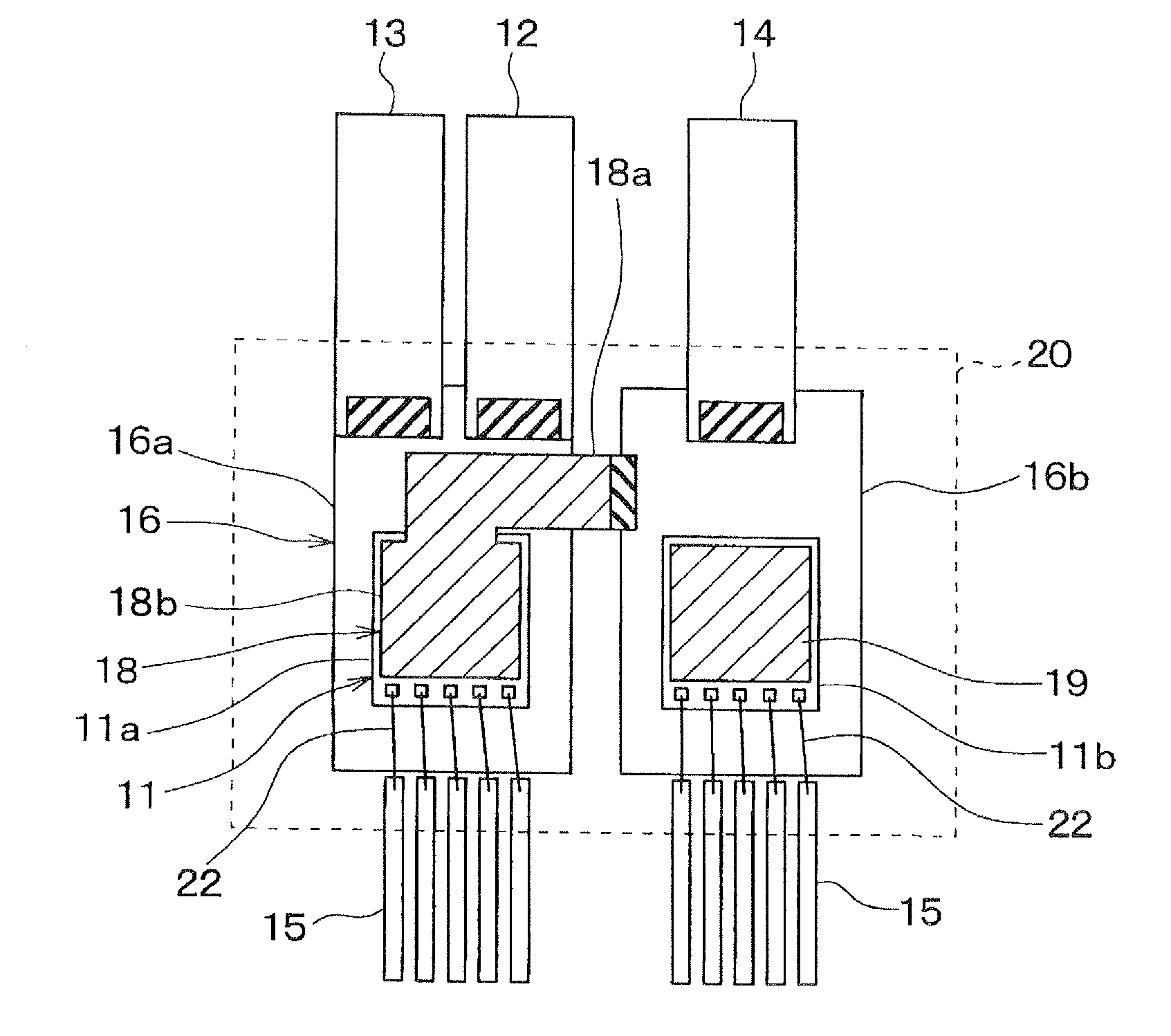
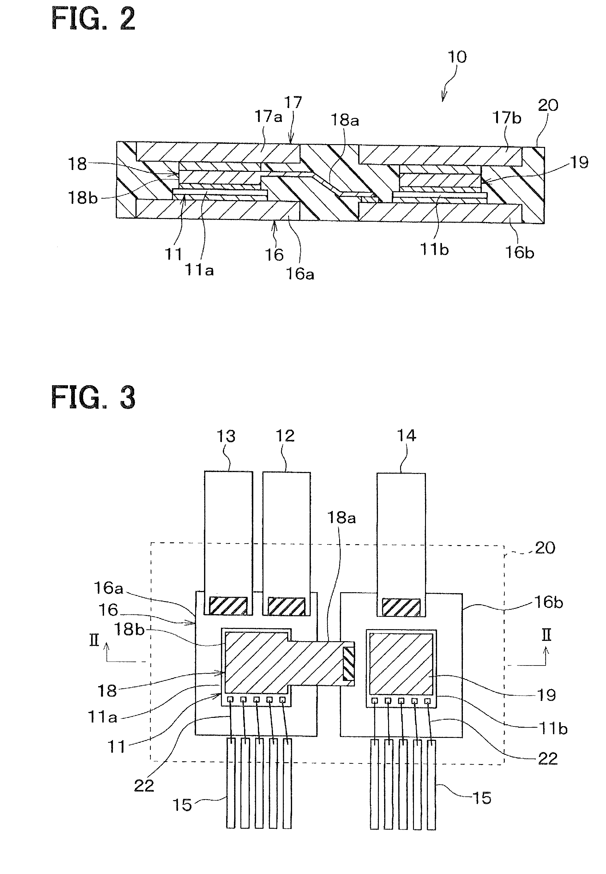
[0112]FIG. 4 is a schematic plan view of the semiconductor module 10, before being molded with the resin, for illustrating the layout of the components. Although FIG. 4 is not a cross-sectional view, some portions are hatched for the sake of clarity. For example, the terminals 18, 19 are hatched with thin lines, and the bonding portions between the leads 12 through 14 and the heat sinks 16, 17 and the bonding portion between the connecting part 18a and the heat sink 16b are hatched with thick lines.

[0113]As shown in FIG. 4, the connecting part 18a is arranged in a different manner from that of the first embodiment shown in FIG. 3. I...

third embodiment

[0115]A third embodiment will be described with reference to FIG. 5. In the semiconductor module 10 according to the present embodiment, the structure of the connecting part 18a is modified from that of the first and second embodiments. Other structures are similar to those of the first and second embodiments, and thus a different structure will be mainly described hereinafter.

[0116]FIG. 5 is a cross-sectional view of the semiconductor module 10. In the first and second embodiments, the connecting part 18a is partly inclined relative to the terminal body portion 18b and connected to the front surface of the heat sink 16b. In the present embodiment, the connecting part 18a is bent, that is, inclined relative to the terminal body portion 18b, and the end of the connecting part 18a is connected to the side surface of the heat sink 16b.

[0117]In this way, the end of the connecting part 18a can be connected to the side surface of the heat sink 16b. In this case, the dimensional tolerance...

fourth embodiment

[0118]A fourth embodiment will be described with reference to FIG. 6. In the semiconductor module 10 according to the present embodiment, the terminal 18 including the connecting part 18a is integral with the middle lead 13. Other structures are similar to those of the first and second embodiments, and a different structure will be mainly described hereinafter.

[0119]FIG. 6 is a schematic plan view of the semiconductor module 10, before being molded with the resin, for illustrating the layout of components. Although FIG. 6 is not a cross-sectional view, some portions are hatched for the sake of clarity.

[0120]As shown in FIG. 6, the middle lead 13 includes a connecting part 13a, an output terminal portion 13b and a terminal body portion 13c. That is, the middle lead 13 is configured to serve as the connecting part, the output terminal and the terminal body portion. In other words, the terminal 18 and the connecting part 18a of the first and second embodiments are integrated with the m...


PUM


Abstract

In a semiconductor module, a first heat sink is disposed on a rear surface of a first semiconductor chip constituting an upper arm, and a second heat sink is disposed on a front surface of the first semiconductor chip through a first terminal. A third heat sink is disposed on a rear surface of a second semiconductor chip constituting a lower arm, and a fourth heat sink is disposed on a front surface of the second semiconductor chip through a second terminal. A connecting part for connecting between the upper arm and the lower arm is integral with the first terminal, and is connected to the third heat sink while being inclined relative to the first terminal.

Description

CROSS REFERENCE TO RELATED APPLICATION[0001]This application is based on Japanese Patent Applications No. 2010-153125 filed on Jul. 5, 2010 and No. 2010-155872 filed on Jul. 8, 2010, the disclosure of which are incorporated herein by reference.FIELD OF THE INVENTION[0002]The present invention relates to a semiconductor module in which a semiconductor chip formed with a semiconductor power element and a heat sink are molded with a resin. More particularly, the present invention relates to a semiconductor module in which at least two semiconductor power element, such as an upper arm (high-side element) and a lower arm (low-side element), are molded with a resin.BACKGROUND OF THE INVENTION[0003]For example, Japanese Patent No. 4192396, which corresponds to US2001 / 0033477, describes a semiconductor module in which an upper arm and a lower arm are connected in series. Such a semiconductor module is known as a 2 in 1 package structure. Each of the upper arm and the lower arm has a semicon...

Claims


Application Information

Patent Timeline
Patent Type & Authority Applications(United States)
IPC IPC(8): H01L23/495H01L21/60
CPCH01L23/49524H01L23/49541H01L2924/1305H01L2224/40247H01L2924/30107H01L2924/13055H01L2224/49175H01L2224/291H01L24/29H01L2924/13091H01L2924/014H01L2924/01074H01L2924/01033H01L2924/01023H01L2924/00014H01L2924/01082H01L2924/01029H01L2224/73265H01L2224/73263H01L2224/73221H01L2224/48247H01L2224/33181H01L2224/32245H01L23/49562H01L23/49568H01L23/49575H01L24/32H01L24/33H01L24/34H01L24/48H01L24/73H01L2224/32145H01L2224/45099H01L2924/00012H01L2924/00H01L2924/181H01L24/40H01L2224/40245H01L2224/05553H01L2224/05554H01L2224/371H01L2224/84801H01L2224/83801H01L24/37H01L24/49H01L2224/0603H01L24/84
Inventor FUKUTANI, KEITAMAMITSU, KUNIAKIOOKURA, YASUSHINISHIHATA, MASAYOSHIWADO, HIROYUKISUGIURA, SYUN
Owner DENSO CORP
Why Eureka
Try Eureka