
Solid-state imaging apparatus and imaging system

a technology of solid-state imaging and imaging apparatus, which is applied in the direction of electrical apparatus, semiconductor devices, radio frequency controlled devices, etc., can solve the problems of image distortion, line defects are problematic, and many problems, and achieve the effect of reducing the sensitivity variation between pixels

Active Publication Date: 2012-01-12
CANON KK
View PDF7 Cites 12 Cited by
  • Summary
  • Abstract
  • Description
  • Claims
  • Application Information

AI Technical Summary

Benefits of technology

[0005]As described above, when the solid-state imaging apparatus includes pixels with different photoelectric conversion element areas, the sensitivity varies between the pixels. Hence, an aspect of the present invention provides a technique of reducing the sensitivity variation between pixels in a solid-state imaging apparatus including pixels with different photoelectric conversion element areas.

Problems solved by technology

Several problems are known to arise when bonding the plurality of imaging blocks.
In Japanese Patent Laid-Open No. 2002-90462, line defects are problematic, which are caused by tiling imaging blocks with scanning circuits and the like arranged at the periphery of the pixel array.
In Japanese Patent Laid-Open No. 2002-44522, adjacent pixels on both sides of the gap between imaging blocks is wider than the gap between adjacent pixels in an imaging block, and resultant image distortion poses a problem.

Method used


Image

  • Solid-state imaging apparatus and imaging system
  • Solid-state imaging apparatus and imaging system
  • Solid-state imaging apparatus and imaging system

Examples


Embodiment Construction

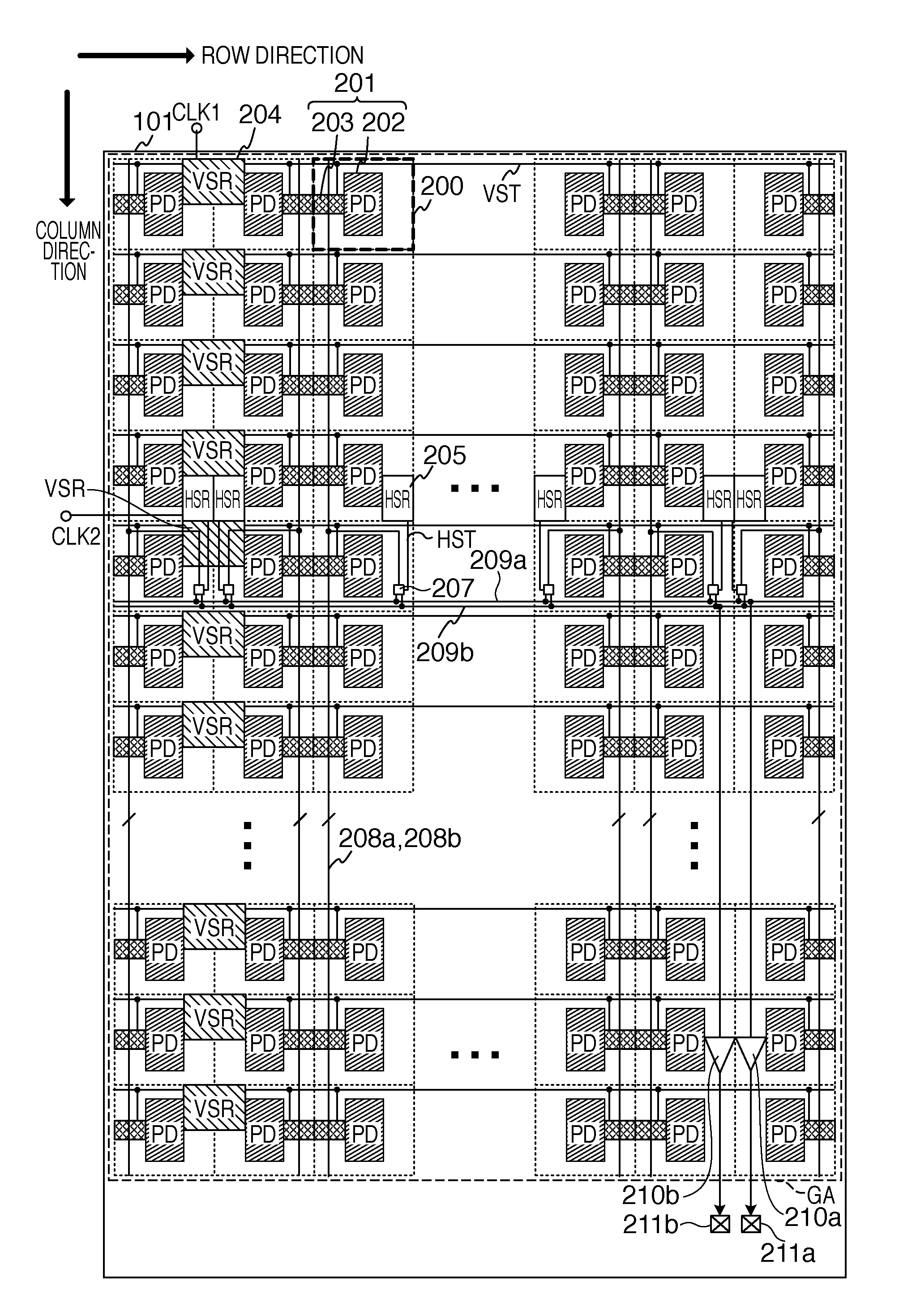
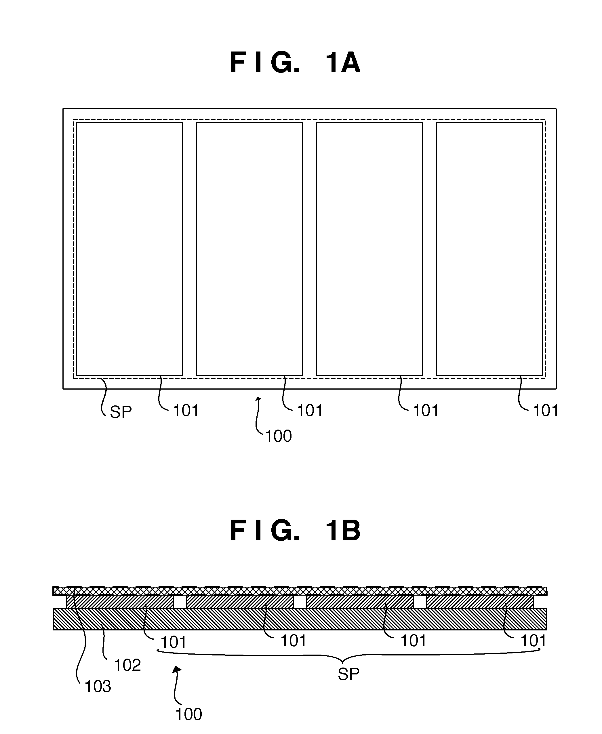
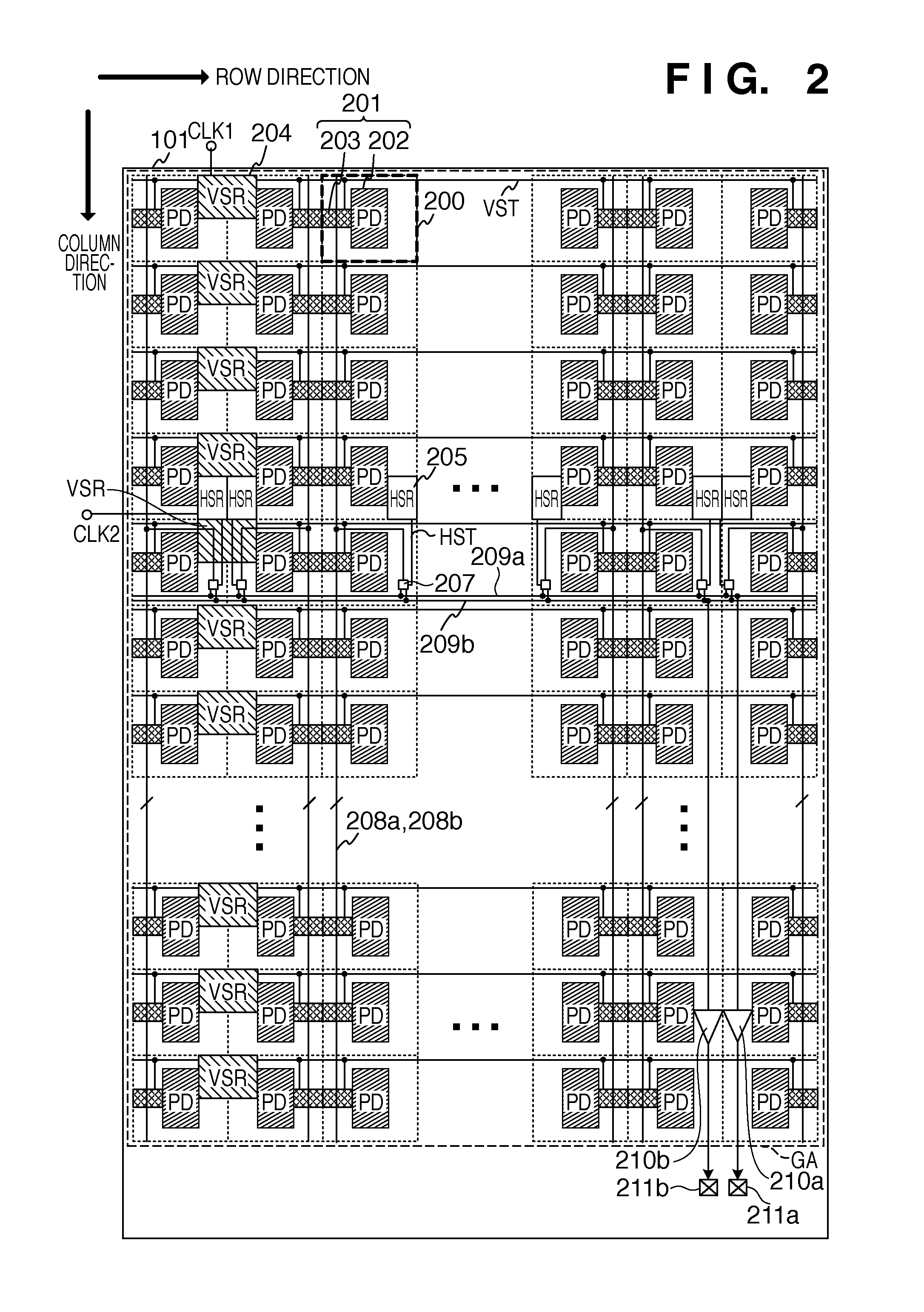
[0018]The schematic arrangement of a solid-state imaging apparatus 100 according to an embodiment of the present invention will be described with reference to FIGS. 1A and 1B. The solid-state imaging apparatus 100 can be formed by, for example, arraying a plurality of imaging blocks 101. In this case, an array of a plurality of imaging blocks 101 can form a sensor panel SP having one imaging region. The plurality of imaging blocks 101 can be arranged on a support substrate 102. When the solid-state imaging apparatus 100 uses a single imaging block 101, the single imaging block 101 forms the sensor panel SP. Each of the plurality of imaging blocks 101 may be provided by, for example, forming a circuit element on a semiconductor substrate or forming a semiconductor layer on, for example, a glass substrate and forming a circuit element on the semiconductor layer. Each of the plurality of imaging blocks 101 has a pixel array in which a plurality of pixels are arrayed so as to form plura...


PUM


Abstract

A solid-state imaging apparatus including pixels each including a photoelectric conversion element, and a light shielding layer covering the photoelectric conversion element is provided. For each of the photoelectric conversion elements, the light shielding layer includes a light shielding portion which shields a portion of incident light to the photoelectric conversion element, and an aperture which passes another portion of the incident light. The pixels include first and second pixels which have different areas on a planar view of the photoelectric conversion element. The area of the photoelectric conversion element in the first pixel is larger than the area of the photoelectric conversion element in the second pixel on the planar view. An area of the light shielding portion included in the first pixel is larger than an area of the light shielding portion included in the second pixel.

Description

BACKGROUND OF THE INVENTION[0001]1. Field of the Invention[0002]The present invention relates to a solid-state imaging apparatus and an imaging system.[0003]2. Description of the Related Art[0004]Sensor panels used in solid-state imaging apparatuses are becoming large in recent years. Along with the upsizing of sensor panels, a technique of tiling a plurality of imaging blocks to implement a large-sized sensor panel has come into general use. Several problems are known to arise when bonding the plurality of imaging blocks. In Japanese Patent Laid-Open No. 2002-90462, line defects are problematic, which are caused by tiling imaging blocks with scanning circuits and the like arranged at the periphery of the pixel array. In this reference, the scanning circuits and the like are arranged in unit cells to solve the problem, as shown in FIG. 7 of this reference. When the scanning circuits and the like are arranged in the unit cells, the area of each unit cell including the scanning circui...

Claims


Application Information

Patent Timeline
Patent Type & Authority Applications(United States)
IPC IPC(8): H01L31/0216
CPCH01L27/14605H01L27/14609H01L31/02164H01L27/14658H01L27/14623H04N25/616H04N25/771H04N25/78
Inventor KONO, SHOJIKIKUCHI, SHINYAMASHITA, YUICHIROFUJIMURA, MASARUSHIMIZU, SHINICHIROARISHIMA, YU
Owner CANON KK
Learn More