Package process of backside illumination image sensor

a backside illumination and image sensor technology, applied in the field of image sensors, can solve the problems of low package efficiency of the package process, limited light sensitive ability of the sensing component, and difficulty in aligning the drilling positions of the holes and the pads, so as to improve package quality, reduce the difficulty of aligning the package process, and reduce the difficulty of the package process

Active Publication Date: 2012-01-12
XENOGENIC DEV LLC
View PDF2 Cites 7 Cited by
  • Summary
  • Abstract
  • Description
  • Claims
  • Application Information

AI Technical Summary

Benefits of technology

[0018]In the package process of the backside illumination image sensor of the present invention, before the wafer is adhered to the first carrier, a plurality of blind vias or a plurality of through holes have been formed. Thus, when the wafer is adhered to the first carrier, only the alignment of the blind vias or the through holes and the pads is needed to be considered. In other words, during forming the through holes, it is not necessary to consider the alignment of the drilling positions of the through holes and the invisible pads. Thus, the alignment difficulty in the package process can be reduced, thereby achieving the exact alignment of the through hole and the pads. As a result, the package efficiency can be increased and the package quality can be improved.

Problems solved by technology

Thus, the light sensitive ability of the sensing component is limited.
Thus, it is difficulty to align of the drilling positions of the holes and the pads.
As a result, the current package process of the backside illumination image sensor has a low the package efficiency.
Furthermore, the inexact alignment of the drilling positions of the holes and the pads will affect the package quality the backside illumination image sensor.

Method used


Image

  • Package process of backside illumination image sensor
  • Package process of backside illumination image sensor
  • Package process of backside illumination image sensor

Examples


Embodiment Construction

[0022]Referring to FIG. 1A to FIG. 1H, FIG. 1A to FIG. 1H illustrate a process flow of a package process of a backside illumination image sensor in accordance with a first embodiment of the present invention.

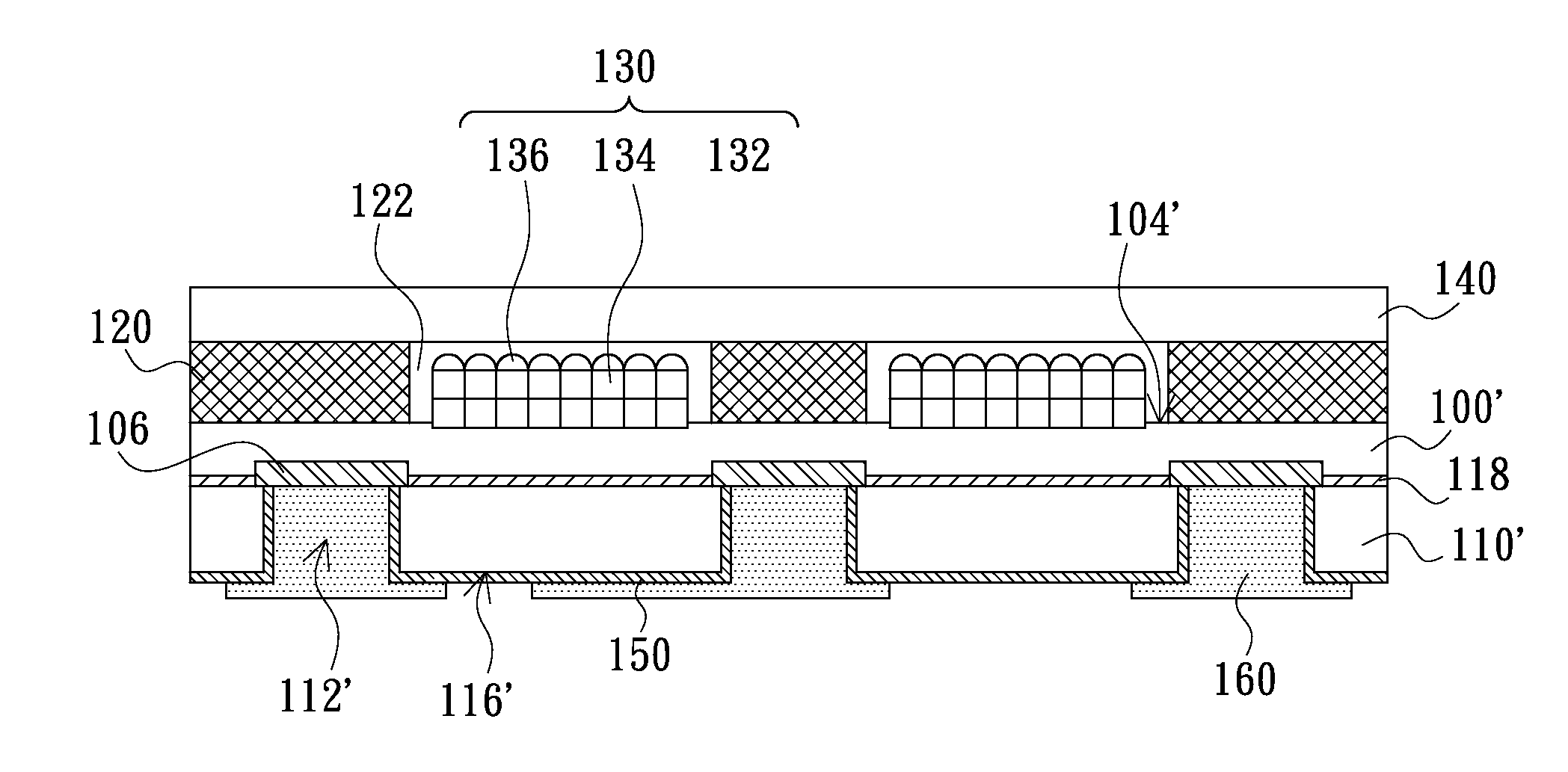
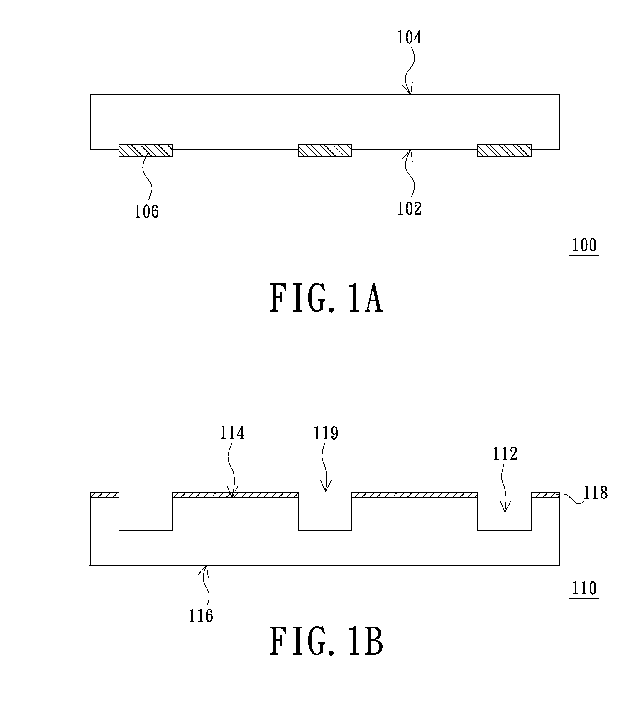
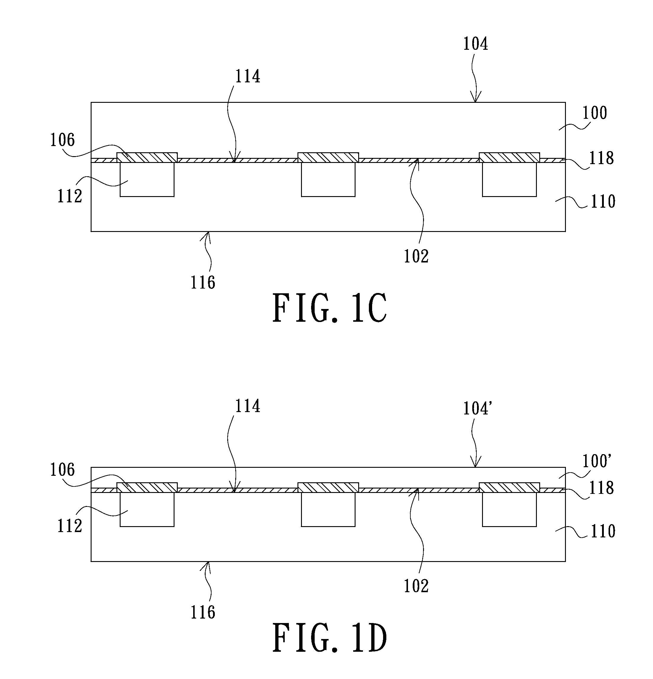
[0023]Referring to FIG. 1A, first, a wafer 100, for example, a semiconductor wafer, is provided. The wafer 100 includes a first surface 102 and a second surface 104 opposite to the first surface 102. The first surface 102 has a plurality of pads 106 disposed thereon.

[0024]Referring to FIG. 1B, next, a first carrier 110 is processed to form a plurality of blind vias 112 therein. In detail, the first carrier 110 is provided. The first carrier 110 includes a front surface 114 and a rear surface 116 opposite to the front surface 114. An oxide layer 118 is formed on the front surface 114 of the first carrier 110. Then, the portions of the oxide layer 118 are removed and the blind vias 112 are formed by using an etching process. In other words, the portions of the oxide layer 118 are ...


PUM


Abstract

In a package process of backside illumination image sensor, a wafer including a plurality of pads is provided. A first carrier is processed to form a plurality of blind vias therein. The first carrier is adhered to the wafer so that the blind vias face to the pads correspondingly. A spacing layer is formed and a plurality of sensing components are disposed. A second carrier is adhered on the spacing layer. Subsequently, a carrier thinning process is performed so that the blind vias become the through holes. An insulating layer is formed on the first carrier. An electrically conductive layer is formed on the insulating layer and filled in the though holes to electrically connect to the pads. The package process can achieve the exact alignment of the through holes and the pads, thereby increasing the package efficiency and improving the package quality.

Description

BACKGROUND[0001]1. Field of the Invention[0002]The present invention relates to an image sensor, and particularly to a package process of a backside illumination image sensor.[0003]2. Description of the Related Art[0004]Image sensor has a function of transforming the received optical signals into the electrical signals, and is widely used in various digital image electronic products. A conventional image sensor includes a semiconductor substrate and a sensing component disposed on the semiconductor substrate. Furthermore, the sensing component is covered by a plurality of metallic circuit layers disposed over the semiconductor substrate. The light entering the conventional image sensor must penetrate the metallic circuit layers before arriving at the sensing component. Thus, the light sensitive ability of the sensing component is limited. Recently, in order to improve the light sensitive ability of the image sensor, a backside illumination image sensor is being researched. The backs...

Claims


Application Information

Patent Timeline
Patent Type & Authority Applications(United States)
IPC IPC(8): H01L21/00
CPCH01L27/1464H01L27/14618H01L27/14632H01L27/14636H01L2924/0002
Inventor CHANG, WEN-HSIUNG
Owner XENOGENIC DEV LLC
Why Eureka
Try Eureka