Image Sensor with Deep Trench Isolation Structure

a technology of image sensor and isolation structure, which is applied in the direction of diodes, semiconductor devices, electrical devices, etc., can solve the problems of insufficient isolation, inability to completely satisfy the user, and the existing bsi image sensor device may begin to suffer from problems,

Active Publication Date: 2012-02-02
TAIWAN SEMICON MFG CO LTD
View PDF5 Cites 136 Cited by
  • Summary
  • Abstract
  • Description
  • Claims
  • Application Information

AI Technical Summary

Problems solved by technology

As transistor device size shrinks with each technology generation, existing BSI image sensor devices may begin to suffer from issues related to cross-talk and blooming.
These issues may be caused by insufficient isolation between n

Method used


Image

  • Image Sensor with Deep Trench Isolation Structure
  • Image Sensor with Deep Trench Isolation Structure
  • Image Sensor with Deep Trench Isolation Structure

Examples


Embodiment Construction

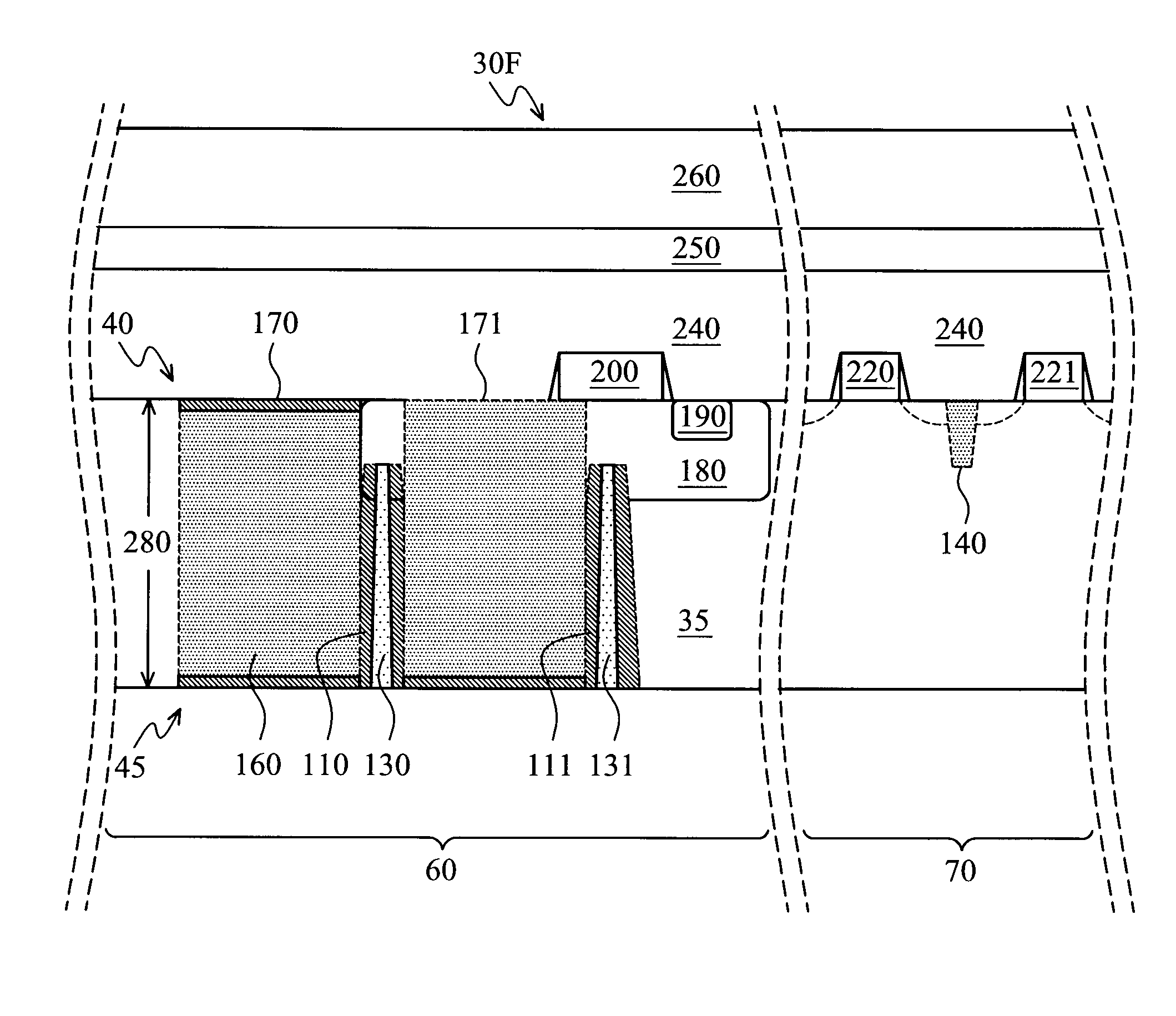
[0008]It is to be understood that the following disclosure provides many different embodiments, or examples, for implementing different features of the invention. Specific examples of components and arrangements are described below to simplify the present disclosure. These are, of course, merely examples and are not intended to be limiting. Moreover, the formation of a first feature over or on a second feature in the description that follows may include embodiments in which the first and second features are formed in direct contact, and may also include embodiments in which additional features may be formed interposing the first and second features, such that the first and second features may not be in direct contact. Various features may be arbitrarily drawn in different scales for the sake of simplicity and clarity.

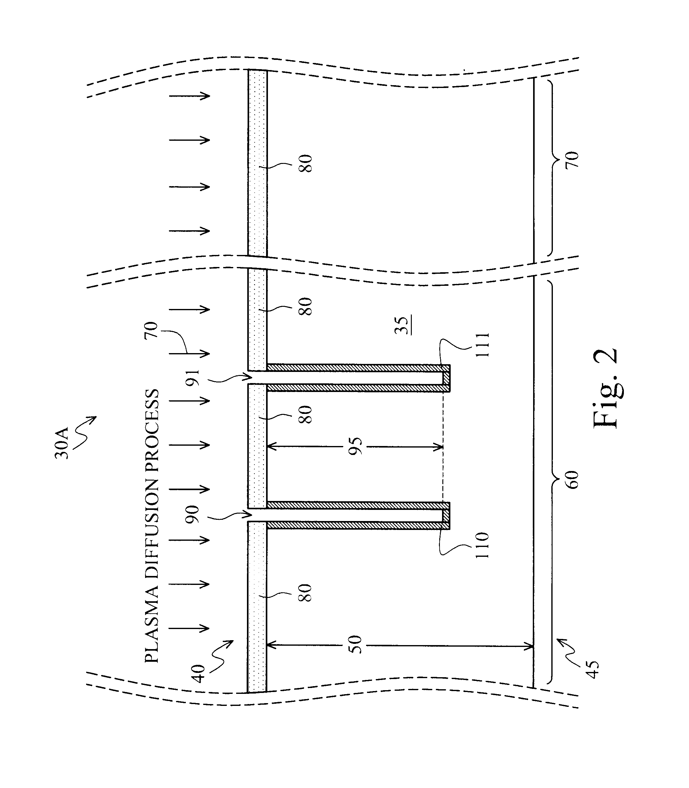
[0009]Illustrated in FIG. 1 is a flowchart of a method 11 for fabricating a back-side illuminated (BSI) image sensor device according to various aspects of the present ...


PUM


Abstract

Provided is a back side illuminated image sensor device. The image sensor device includes a substrate having a front side and a back side opposite the front side. The image sensor also includes a radiation-detection device that is formed in the substrate. The radiation-detection device is operable to detect a radiation wave that enters the substrate through the back side. The image sensor further includes a deep trench isolation feature that is disposed adjacent to the radiation-detection device. The image sensor device further includes a doped layer that at least partially surrounds the deep trench isolation feature in a conformal manner.

Description

BACKGROUND[0001]Semiconductor image sensors are used for sensing light. Complementary metal-oxide-semiconductor (CMOS) image sensors (CIS) and charge-coupled device (CCD) sensors are widely used in various applications such as digital still camera or mobile phone camera applications. These devices utilize an array of pixels in a substrate, including photodiodes and transistors, that can absorb radiation projected toward the substrate and convert the sensed radiation into electrical signals.[0002]A back side illuminated (BSI) image sensor device is one type of image sensor device. As transistor device size shrinks with each technology generation, existing BSI image sensor devices may begin to suffer from issues related to cross-talk and blooming. These issues may be caused by insufficient isolation between neighboring pixels of the BSI image sensor.[0003]Therefore, while existing methods of fabricating BSI image sensor devices have been generally adequate for their intended purposes,...

Claims


Application Information

Patent Timeline
IPC IPC(8): H01L31/02H01L31/0264H01L31/0376H01L31/18
CPCH01L27/1464H01L27/14689H01L27/14643
Inventor CHEN, SZU-YINGCHUANG, CHUN-CHIEHLIU, JEN-CHENGYAUNG, DUN-NIAN
Owner TAIWAN SEMICON MFG CO LTD
Why Eureka
Try Eureka