Vertical division of three-dimensional memory device

a three-dimensional memory, vertical division technology, applied in the direction of semiconductor devices, instruments, electrical devices, etc., can solve the problems of false logic state reading, unreliable reading and writing of data, and scale reduction has started to create problems

Inactive Publication Date: 2017-03-02
CYPRESS SEMICON CORP
View PDF10 Cites 57 Cited by
  • Summary
  • Abstract
  • Description
  • Claims
  • Application Information

AI Technical Summary

Benefits of technology

[0048]FIG. 14 is a block diagram illustrating a cross-sectional view of a portion of vertical NV memory array 200 fabricated according to the method of FIGS. 1 and 2A-13. As illustrated, while the five half vertical NV memory cell strings shown may be operated individually to increase memory bits of the entire array 200, they may share a same set of control gates and / or word lines. In one embodiment, vertical NV memory array 200 may include multiple portions as illustrated in FIG. 14 in which each portion may share a same set of word lines.

Problems solved by technology

The fabrication of two-dimensional or planar flash memory devices is down to 10 nm lithography, and the reduction in scale has started to create issues as each NV memory element is getting smaller and physically closer to one another.
As a result, any small imperfection in the fabrication process may cause logic / memory states of the NV memory elements to become difficult to differentiate, which may result in a false reading of logic states.
Moreover, control electrodes are getting so small and closely spaced that their effects, such as in biasing gates, may spread over more than one memory cells or strings, which may lead to unreliable reading and writing of data.

Method used


Image

  • Vertical division of three-dimensional memory device
  • Vertical division of three-dimensional memory device
  • Vertical division of three-dimensional memory device

Examples


Embodiment Construction

[0020]The following description sets forth numerous specific details such as examples of specific systems, components, methods, and so forth, in order to provide a good understanding of several embodiments of the present subject matter. It will be apparent to one skilled in the art, however, that at least some embodiments may be practiced without these specific details. In other instances, well-known components or methods are not described in detail or are presented in a simple block diagram format in order to avoid unnecessarily obscuring the techniques described herein. Thus, the specific details set forth hereinafter are merely exemplary. Particular implementations may vary from these exemplary details and still be contemplated to be within the spirit and scope of the present subject matter.

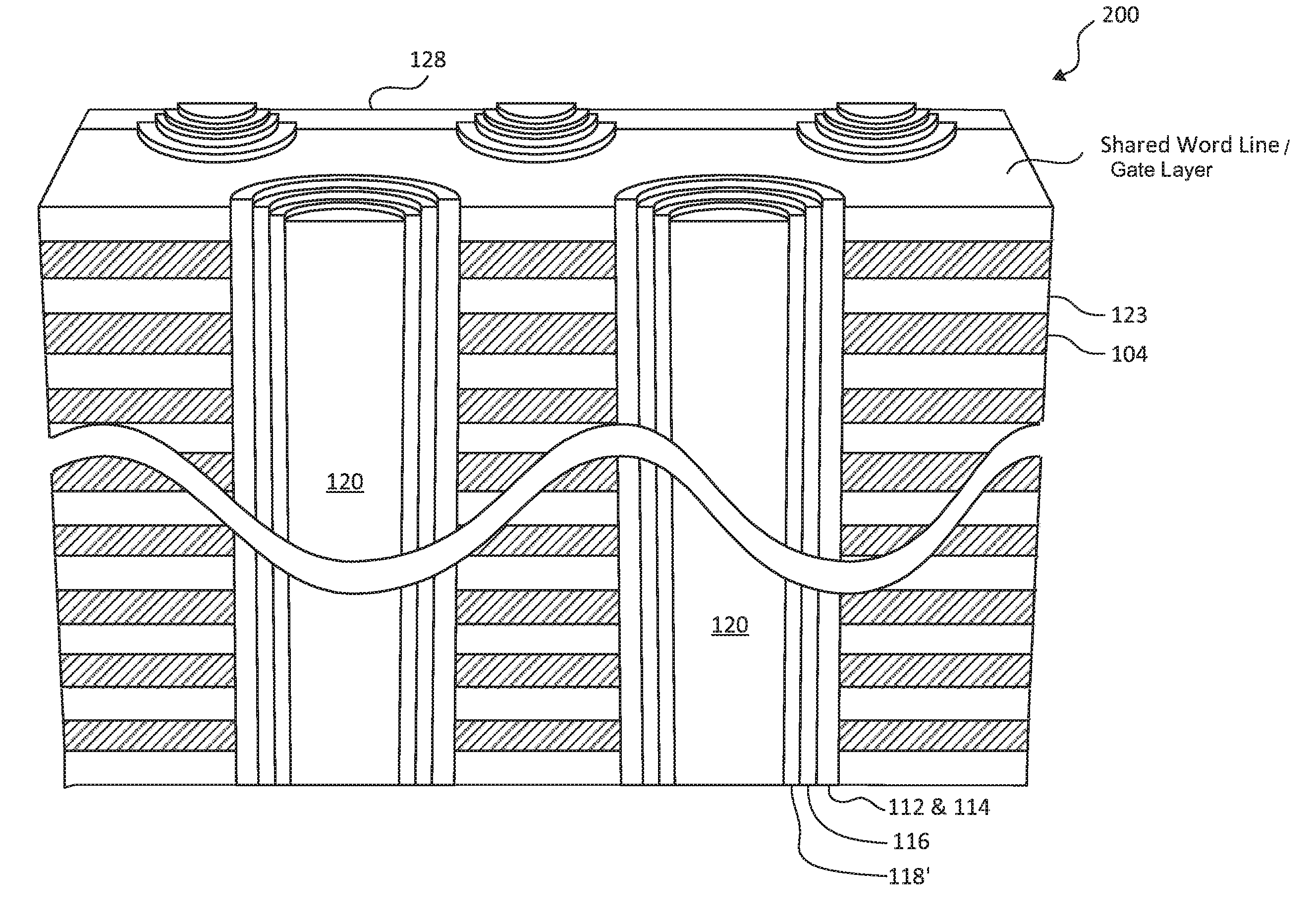
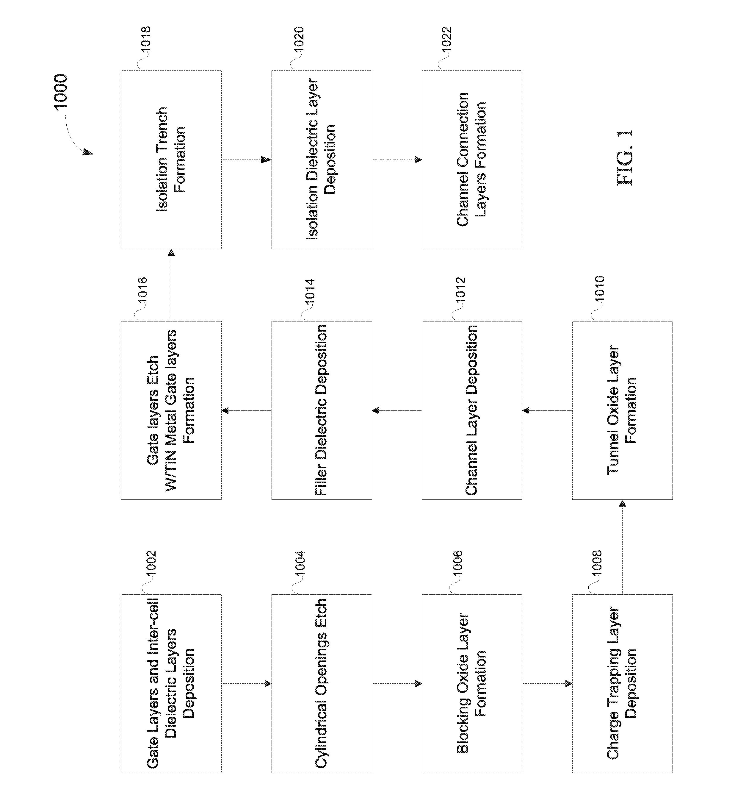
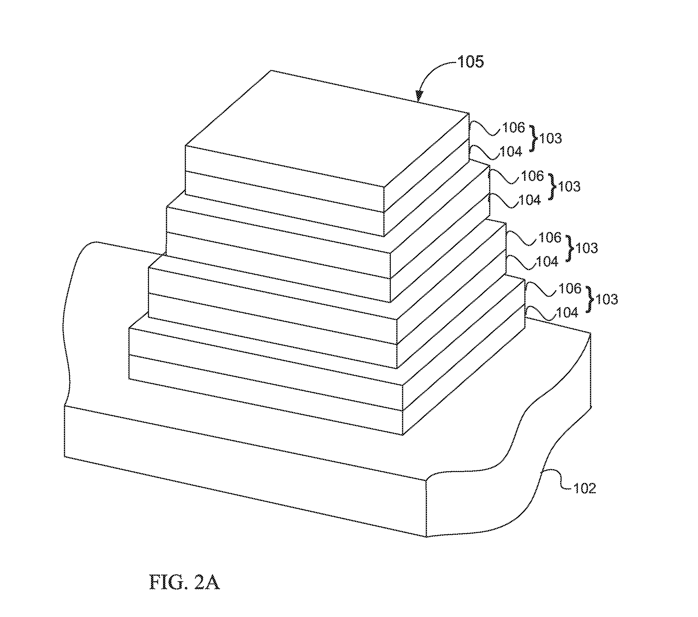
[0021]Embodiments of a vertical or three-dimensional (3D) non-volatile (NV) memory device including strings of non-volatile memory (NVM) transistors and / or field-effect transistors (FET), and ...


PUM


Abstract

A method of forming a vertical non-volatile (NV) memory device such as 3-D NAND flash memory includes forming a vertical NV memory cell string within an opening disposed in a stack of alternating layers of a first layer and a second layer over a substrate, and dividing the vertical NV memory cell string into two halves with a first vertical deep trench and an isolation dielectric pillar formed in the first vertical deep trench, such that memory bit density of the divided vertical NV memory cell strings double the memory bits of the device.

Description

PRIORITY[0001]The present application claims the priority and benefit under 35 U.S.C. §119(e) of U.S. Provisional Application No. 62 / 212,220, filed on Aug. 31, 2015, which is incorporated by reference herein in its entirety.TECHNICAL FIELD[0002]The present disclosure relates generally to non-volatile (NV) memory devices, and more particularly to three-dimensional (3D) or vertical NV memory cell strings and methods of manufacturing thereof including dividing vertical memory cell strings to enhance memory bit density and integrity.BACKGROUND[0003]Flash memory, both the NAND and NOR types, includes strings of NV memory elements or cells, such as floating-gate metal-oxide-semiconductor field-effect (FGMOS) transistors and silicon-oxide-nitride-oxide-silicon (SONOS) transistors. The fabrication of two-dimensional or planar flash memory devices is down to 10 nm lithography, and the reduction in scale has started to create issues as each NV memory element is getting smaller and physically ...

Claims


Application Information

Patent Timeline
Patent Type & Authority Applications(United States)
IPC IPC(8): H01L27/115G11C16/04
CPCH01L27/11582H01L27/11565G11C16/0483H10B43/10H10B43/35H10B43/27H01L21/3065H01L21/76205H01L21/0228H10B41/20H10B43/20H10B41/27H10B43/30H10B41/30
Inventor SUGINO, RINJIBELL, SCOTTXUE, LEI
Owner CYPRESS SEMICON CORP
Why Eureka
Try Eureka