Soi deep trench capacitor employing a non-conformal inner spacer

a capacitor and inner spacer technology, applied in the field of deep trench capacitors, can solve the problems of increasing processing complexity and cost, and achieve the effect of simplifying and cost-effective manufacturing sequences

Inactive Publication Date: 2009-11-26
GLOBALFOUNDRIES INC
View PDF8 Cites 57 Cited by
  • Summary
  • Abstract
  • Description
  • Claims
  • Application Information

AI Technical Summary

Benefits of technology

[0008]The present invention addresses the needs described above by providing a semiconductor structure comprising a bottle shaped trench capacitor in a semiconductor-on-insulator (SOI) substrate and a simplified and cost-effective manufacturing sequence for the same.

Problems solved by technology

Further, protection of portions of the top semiconductor layer adjoining the deep trench requires multiple additional processing steps, thereby increasing processing complexity and cost

Method used


Image

  • Soi deep trench capacitor employing a non-conformal inner spacer
  • Soi deep trench capacitor employing a non-conformal inner spacer
  • Soi deep trench capacitor employing a non-conformal inner spacer

Examples


first embodiment

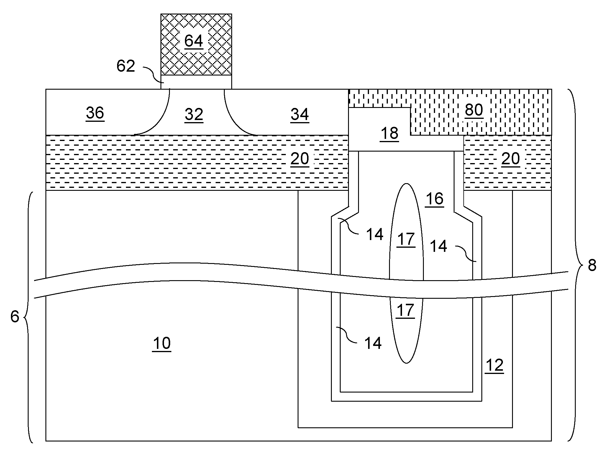
[0064]Referring to FIG. 1, a first exemplary semiconductor structure according to the present invention comprises a semiconductor-in-insulator (SOI) substrate 8 containing a top semiconductor layer 30, a buried insulator layer 20, and a bottom semiconductor layer 6. Each of the top semiconductor layer 30 and the bottom semiconductor layer 6 comprises a semiconductor material. The semiconductor material of the top semiconductor layer 30 and the semiconductor material of the bottom semiconductor layer 6 may be the same, or different. The semiconductor materials for the top semiconductor layer 30 and the bottom semiconductor layer 6 may be selected from, but are not limited to, silicon, germanium, silicon-germanium alloy, silicon carbon alloy, silicon-germanium-carbon alloy, gallium arsenide, indium arsenide, indium phosphide, III-V compound semiconductor materials, II-VI compound semiconductor materials, organic semiconductor materials, and other compound semiconductor materials. Typi...

second embodiment

[0090]Referring to FIG. 12, a second exemplary semiconductor structure according to the present invention is derived from the first exemplary semiconductor structure of FIG. 1 by depositing a conformal dielectric diffusion barrier layer 42L. The conformal dielectric diffusion barrier layer 42L comprises a dielectric material that functions as a diffusion barrier layer for electrical dopant ions such as B, Ga, In, P, As, and Sb. The conformal dielectric diffusion barrier layer 42L may comprise a dielectric nitride, a dielectric oxide, a dielectric oxynitride, or a combination thereof. An exemplary material for the conformal dielectric diffusion barrier layer 42L.

[0091]The conformal dielectric diffusion barrier layer 42L is deposited by chemical vapor deposition (CVD) such as low pressure chemical vapor deposition (LPCVD), rapid thermal chemical vapor deposition (RTCVD), atomic layer deposition (ALD), etc. The conformal dielectric diffusion barrier layer 42L is conformal so that the t...


PUM


Abstract

A bottle shaped trench for an SOI capacitor is formed by a simple processing sequence. A non-conformal dielectric layer with an optional conformal dielectric diffusion barrier layer underneath is formed on sidewalls of a deep trench. Employing an isotropic etch, the non-conformal dielectric layer is removed from a bottom portion of the deep trench, leaving a dielectric spacer covering sidewalls of the buried insulator layer and the top semiconductor layer. The bottom portion of the deep trench is expanded to form a bottle shaped trench, and a buried plated is formed underneath the buried insulator layer. The dielectric spacer may be recessed during formation of a buried strap to form a graded thickness dielectric collar around the upper portion of an inner electrode. Alternately, the dielectric spacer may be removed prior to formation of a buried strap.

Description

FIELD OF THE INVENTION[0001]The present invention relates to a semiconductor structure, and particularly to a deep trench capacitor in a semiconductor-on-insulator (SOI) substrate employing a non-conformal inner spacer, and methods of manufacturing the same.BACKGROUND OF THE INVENTION[0002]Deep trench capacitors are used in a variety of semiconductor chips for high areal capacitance and low device leakage. Typically, a deep trench capacitor provides a capacitance in the range from about 4 fF (femto-Farad) to about 120 fF. A deep trench capacitor may be employed as a charge storage unit in a dynamic random access memory (DRAM), which may be provided as a stand-alone semiconductor chip, or may be embedded in a system-on-chip (SoC) semiconductor chip. A deep trench capacitor may also be employed in a variety of circuit applications such as a charge pump or a capacitive analog component in a radio-frequency (RF) circuit.[0003]Semiconductor-on-insulator (SOI) devices formed on an SOI sub...

Claims


Application Information

Patent Timeline
Patent Type & Authority Applications(United States)
IPC IPC(8): H01L29/94H01L21/20
CPCH01L21/84H01L27/1087H01L29/945H01L29/66181H01L27/1203H10B12/0387
Inventor CHENG, KANGGUOHO, HERBERT L.PARRIES, PAUL C.WANG, GENG
Owner GLOBALFOUNDRIES INC
Why Eureka
Try Eureka