Three-dimensional Memory Device and Manufacturing Method Thereof

a three-dimensional memory and manufacturing method technology, applied in the direction of semiconductor devices, basic electric elements, electrical appliances, etc., can solve the problems of low read-write efficiency, difficult operation of multi-level cells, and large process complexity, so as to improve integration density, simplify the etching process of stacked structures, and maintain the control performance of metal gates

Active Publication Date: 2017-08-17
INST OF MICROELECTRONICS CHINESE ACAD OF SCI
View PDF5 Cites 57 Cited by
  • Summary
  • Abstract
  • Description
  • Claims
  • Application Information

AI Technical Summary

Benefits of technology

[0021]In accordance with the three-dimensional memory manufacturing method of the present invention, the deep trenches of word-line in the TCAT three-dimensional device are replaced with deep-hol

Problems solved by technology

As the size of the memory cells of the two-dimensional (2D) memory devices continues to shrink, signal conflict and interference will increase so significantly that it is difficult to perform operation of multi-level cell (MLC).
Meanwhile, the etching for both of the deep trenches and the deep hole channels are etching for multilayer stack, with great process complexity, and the shape difference from deep holes to deep trenches requires the change of the etching proce

Method used


Image

  • Three-dimensional Memory Device and Manufacturing Method Thereof
  • Three-dimensional Memory Device and Manufacturing Method Thereof
  • Three-dimensional Memory Device and Manufacturing Method Thereof

Examples


Embodiment Construction

[0024]The features and technical effects of the present invention will be described in detail with reference to the drawings and schematic embodiments, disclosing an innovative method for manufacturing 3-D memory structure which can realize contact interconnection with low cost and maintain the control performance of the metal gate. It should be noted that the similar reference numbers denote the similar structure. The terms used in the present invention like “first”, “second”, “up / upon”, “down / low / beneath / under” etc. can be used in denoting various device structures, and do not indicate the relationship in space, sequence or hierarchy of the device structures unless specially illuminated these terms, if not stated otherwise.

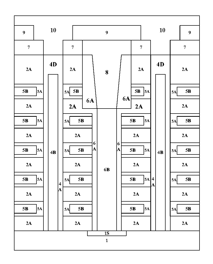
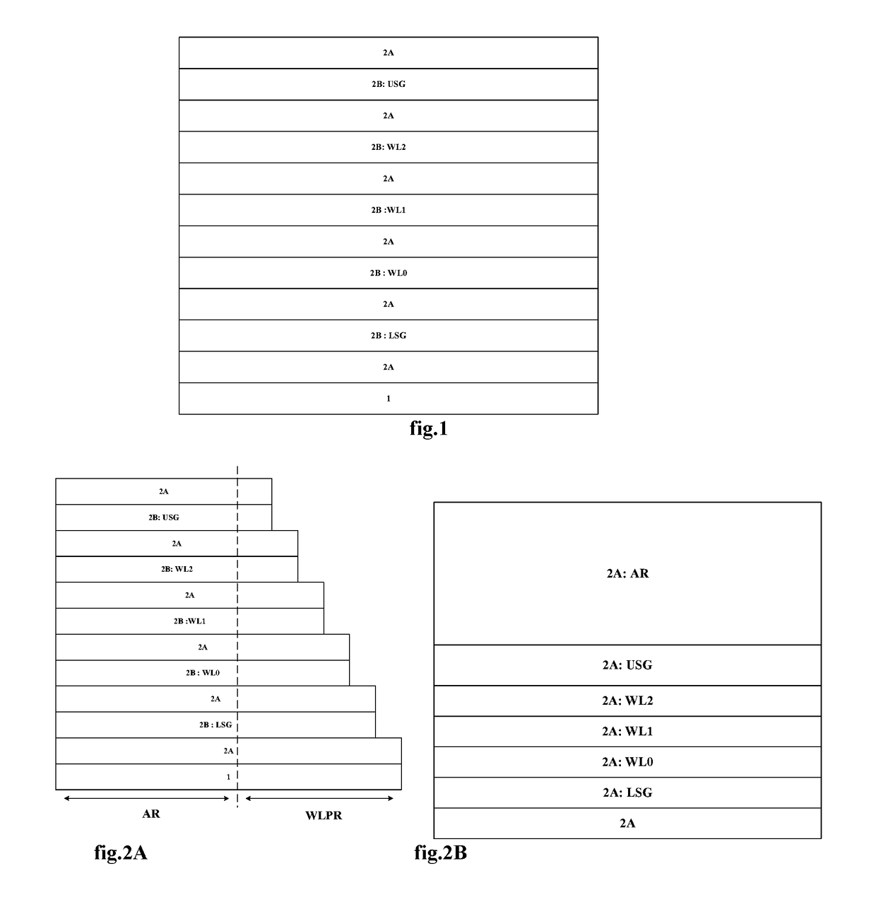
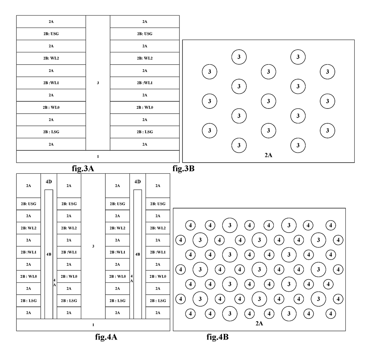
[0025]As shown in FIG. 1, a stack structure 2 composed of a plurality of first material layers 2A and a plurality of second material layers 2B is formed alternately on the substrate 1. The material of substrate 1 may comprise bulk silicon (bulk Si), bulk germani...


PUM


Abstract

A method for manufacturing three-dimensional memory, comprising the steps of: forming a stack structure composed of a plurality of first material layers and a plurality of second material layers on a substrate; etching the stack structure to expose the substrate, forming a plurality of first vertical openings; forming a filling layer in each of the first openings; etching the stack structure around each of the first openings to expose the substrate, forming a plurality of second vertical openings; forming a vertical channel layer and a drain in each of the second openings; removing the filling layer by selective etching, re-exposing the first openings; partially or completely removing the second material layers by lateral etching, leaving a plurality of recesses; forming a plurality of gate stack structure in the recesses; forming a plurality of common sources on and/or in the substrate at the bottom of each of the first openings. In accordance with the three-dimensional memory manufacturing method of the present invention, the deep trenches of word-line in the TCAT three-dimensional device are replaced with deep-hole etching to realize the same function, thereby improving the integration density, simplifying the etching process of stacked structure, and maintaining the control performance of the metal gate.

Description

[0001]This application is a National Phase application of, and claims priority to, PCT Application No. PCT / CN2014 / 087478, filed on Sep. 25, 2014, entitled “Three-dimensional memory device and manufacturing method thereof”, which claimed priority to Chinese Application No. 201410404550.X, filed on Aug. 15, 2014. Both the PCT Application and Chinese Application are incorporated herein by reference in their entireties.TECHNICAL FIELD[0002]The present invention relates to a semiconductor device and manufacturing method thereof, particularly to a high-density three-dimensional memory device and manufacturing method thereof.BACKGROUND TECHNIQUE[0003]In order to improve the density of the memory device, the industry has worked extensively at developing a method for reducing the size of a two-dimensional arrangement of memory cells. As the size of the memory cells of the two-dimensional (2D) memory devices continues to shrink, signal conflict and interference will increase so significantly ...

Claims


Application Information

Patent Timeline
IPC IPC(8): H01L27/11582
CPCH01L27/11582H01L28/00H10B43/27H10B43/20
Inventor HUO, ZONGLIANGLIU, MINGJIN, LEI
Owner INST OF MICROELECTRONICS CHINESE ACAD OF SCI
Why Eureka
Try Eureka