Method to improve charge pump reliability, efficiency and size

a technology of capacitor dielectric and reliability, applied in the direction of electric variable regulation, process and machine control, instruments, etc., can solve the problems of capacitor dielectric used in "high-stress" circuits, oxide reliability concerns becoming more and more severe, and dielectric breakdown of capacitor dielectrics

Inactive Publication Date: 2003-09-11
INFINEON TECHNOLOGIES NORTH AMERICA CORPORATION
View PDF0 Cites 59 Cited by
  • Summary
  • Abstract
  • Description
  • Claims
  • Application Information

AI Technical Summary

Problems solved by technology

In semiconductor capacitor structures, oxide reliability concern becomes more and more severe as the oxide thickness is further scaled down.
Capacitor dielectric used in "high-stress" circuits could suffer dielectric breakdown if the devices are not properly protected.

Method used


Image

  • Method to improve charge pump reliability, efficiency and size
  • Method to improve charge pump reliability, efficiency and size
  • Method to improve charge pump reliability, efficiency and size

Examples


Embodiment Construction

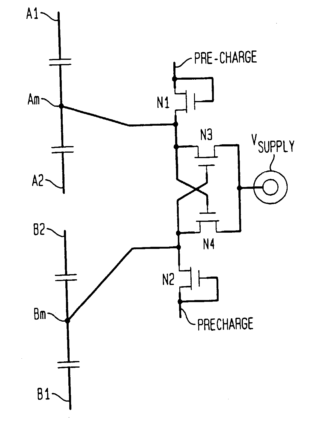
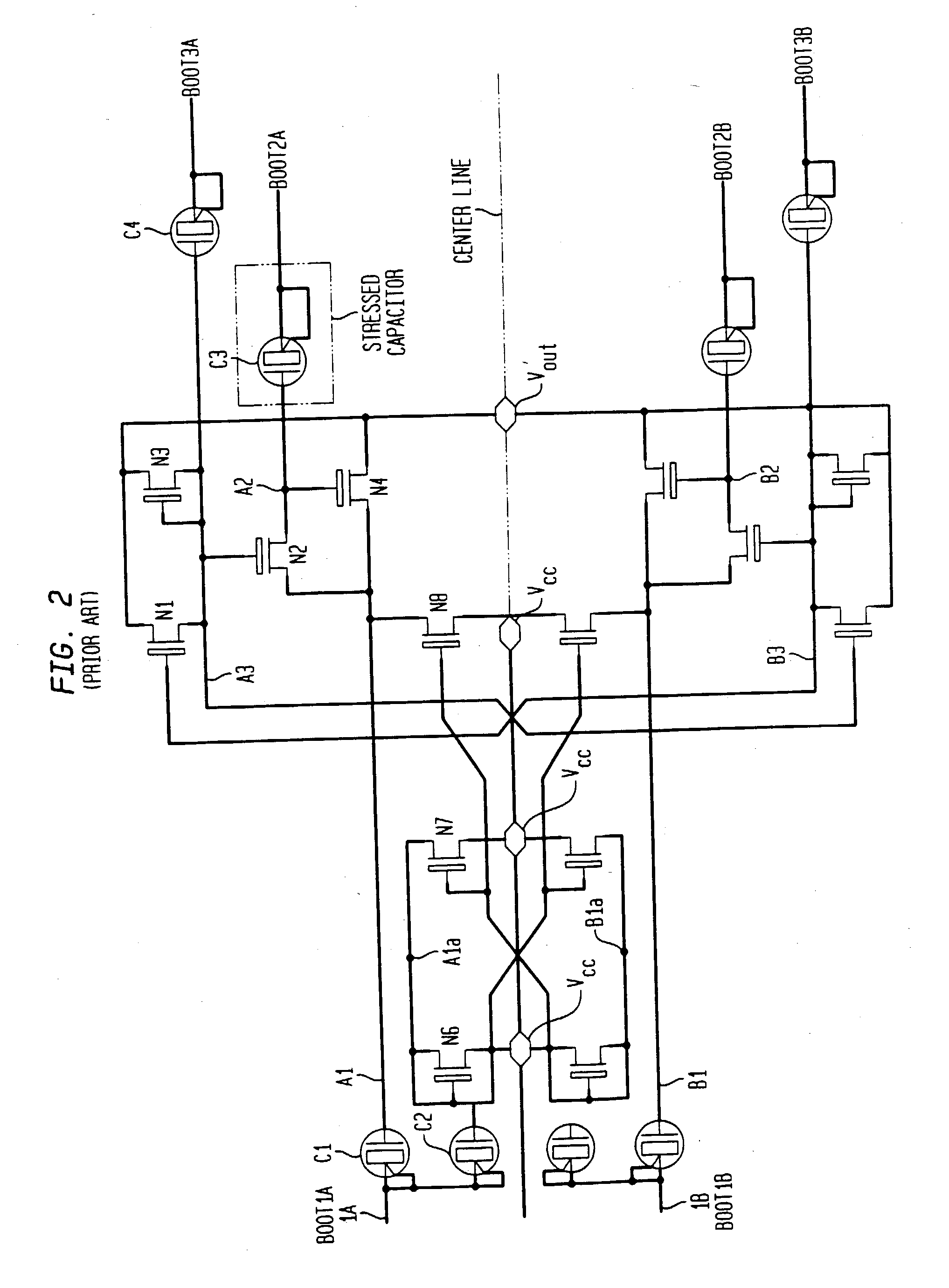
[0023] The invention is a method to prevent dielectric breakdown of semiconductor capacitor structures under excessive voltage stress. More specifically, the method according to the invention prevents dielectric break down of boost capacitors of a charge pump circuit as an example. A modem charge pump is illustrated in FIG. 2. Usually several different sized capacitors, C1, C2, C3, C4, etc., are used to boost the output voltage efficiently. The capacitor size varies from 50 Fm.sup.2 to 4500 Fm.sup.2. Normally, in each DRAM chip, up to forty pumps may be employed. Therefore, the overall stress area can be significant, and the breakdown probability is relatively high.

[0024] The pump has a symmetrical design. The upper portion of the circuit and the lower portion of the circuit are mirrored to the center line. An oscillator and a timing circuit (not shown) are used to generate the clocked boosted signals, BOOTA, BOOTB, etc. During the first half clock period, the upper portion of the c...


PUM


Abstract

A dynamic clamp is used in conjunction with capacitors with thinner dielectric or with deep trench capacitors to solve the problem of dielectric breakdown in high stress capacitors. The dynamic clamp is realized using a two stage pump operation cycle such that, during a first stage pump cycle, a middle node of a pair of series connected capacitors is pre-charged to a supply voltage and, during a second stage pump cycle, the middle node is coupled by a boost clock. Thus, at any moment in the pump operation cycle, the voltage across the capacitors is held within a safety range.

Description

DESCRIPTION[0001] 1. Field of the Invention[0002] The present invention generally relates to semiconductor structures and, more particularly, to a method to design a low-cost, high-performance charge pump system.[0003] 2. Background Description[0004] In semiconductor capacitor structures, oxide reliability concern becomes more and more severe as the oxide thickness is further scaled down. Capacitor dielectric used in "high-stress" circuits could suffer dielectric breakdown if the devices are not properly protected. A general guideline for the dielectric reliability is shown in FIG. 1. If the thickness of the dielectric for a technology is chosen to be 55 nm (the vertical dash line), then for gate or capacitor devices with 10 mm.sup.2 area can sustain a voltage V1 (about 2.2 volts) maximum use voltage without having a reliability concern. The smaller the over-all device area, the higher sustainable stress voltage is allowed for the device. On the other hand, the thinner the dielectri...

Claims


Application Information

Patent Timeline
Patent Type & Authority Applications(United States)
IPC IPC(8): G11C5/14
CPCG11C5/145
Inventor HSU, LOUISHOUGHTON, RUSSELL J.WEINFURTNER, OLIVER
Owner INFINEON TECHNOLOGIES NORTH AMERICA CORPORATION
Why Eureka
Try Eureka