Metal semiconductor alloy structure for low contact resistance

a metal semiconductor alloy and low contact resistance technology, applied in the direction of semiconductor devices, semiconductor/solid-state device details, electrical devices, etc., can solve the problems of adversely affecting device performance, limited volume of metal semiconductor alloy formed by anneal,

Inactive Publication Date: 2012-02-09
IBM CORP
View PDF7 Cites 131 Cited by
  • Summary
  • Abstract
  • Description
  • Claims
  • Application Information

AI Technical Summary

Problems solved by technology

Thus, the volume of the metal semiconductor alloy formed by the anneal is limited by the area of the contact between the metal layer and the underlying semiconductor material.
However, a high contact resistance of a metal semiconductor alloy region adversely impacts device performance by introducing extra parasitic resistance.

Method used


Image

  • Metal semiconductor alloy structure for low contact resistance
  • Metal semiconductor alloy structure for low contact resistance
  • Metal semiconductor alloy structure for low contact resistance

Examples


Embodiment Construction

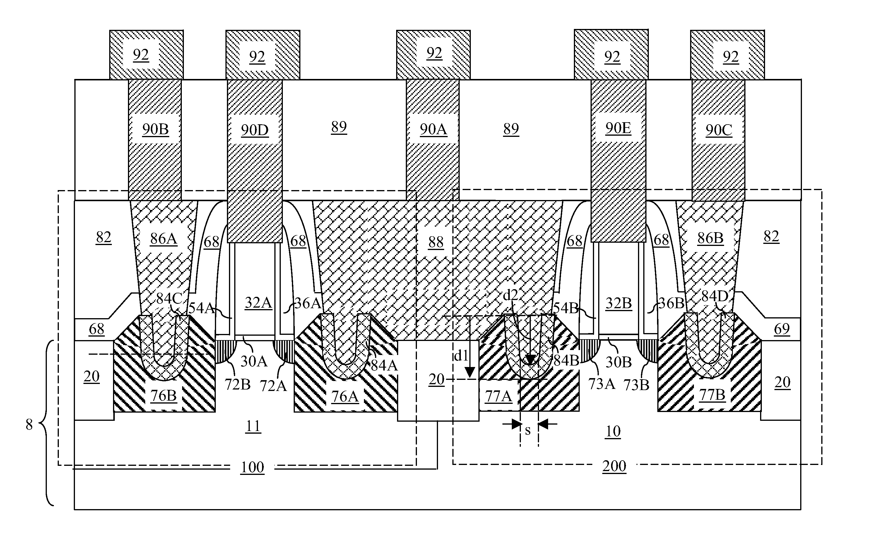
[0028]As stated above, the present disclosure relates to metal semiconductor alloy structures for providing low contact resistance and methods of forming the same, which are now described in detail with accompanying figures. It is noted that like and corresponding elements are referred to by like reference numerals across the various drawings.

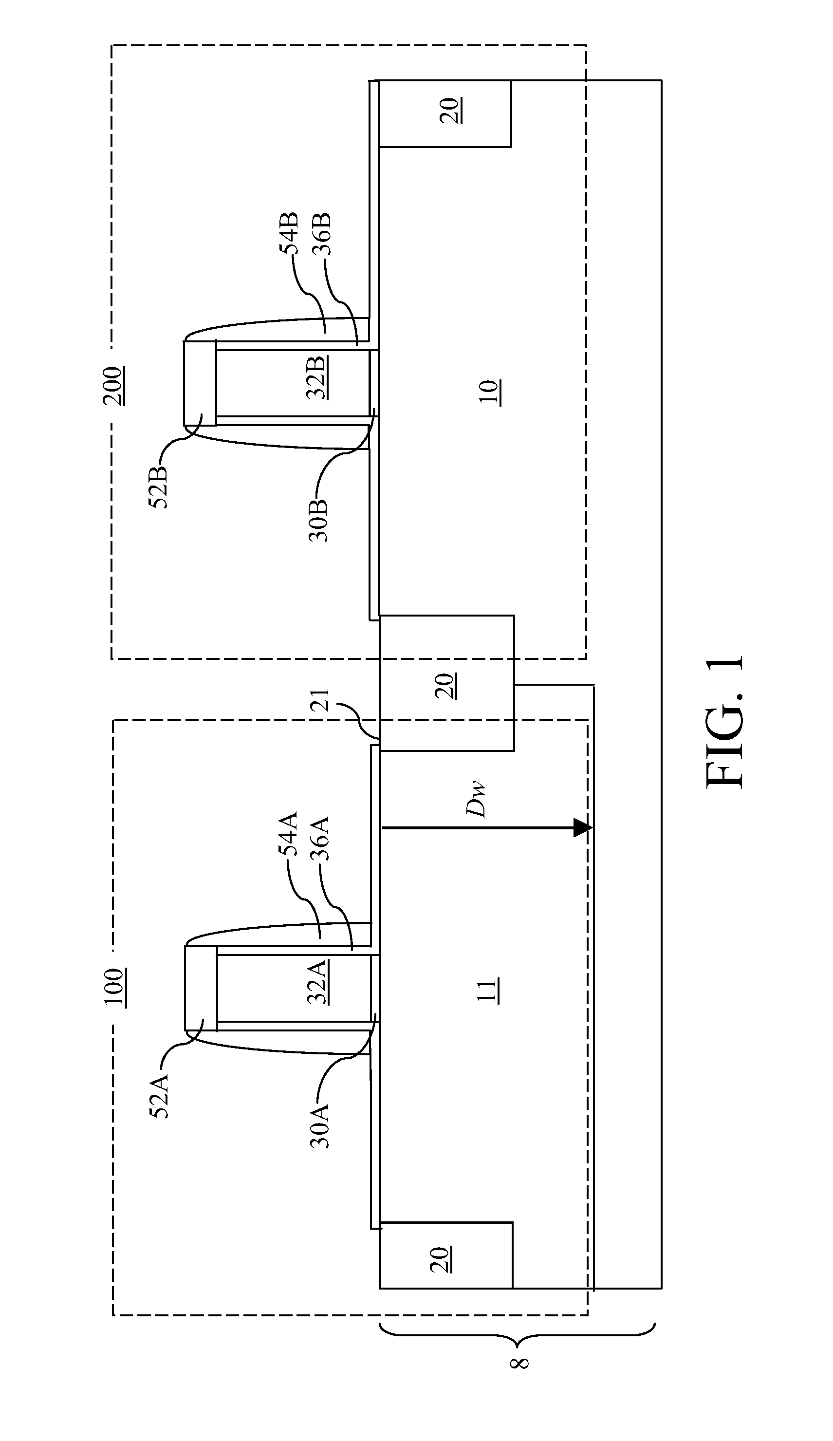
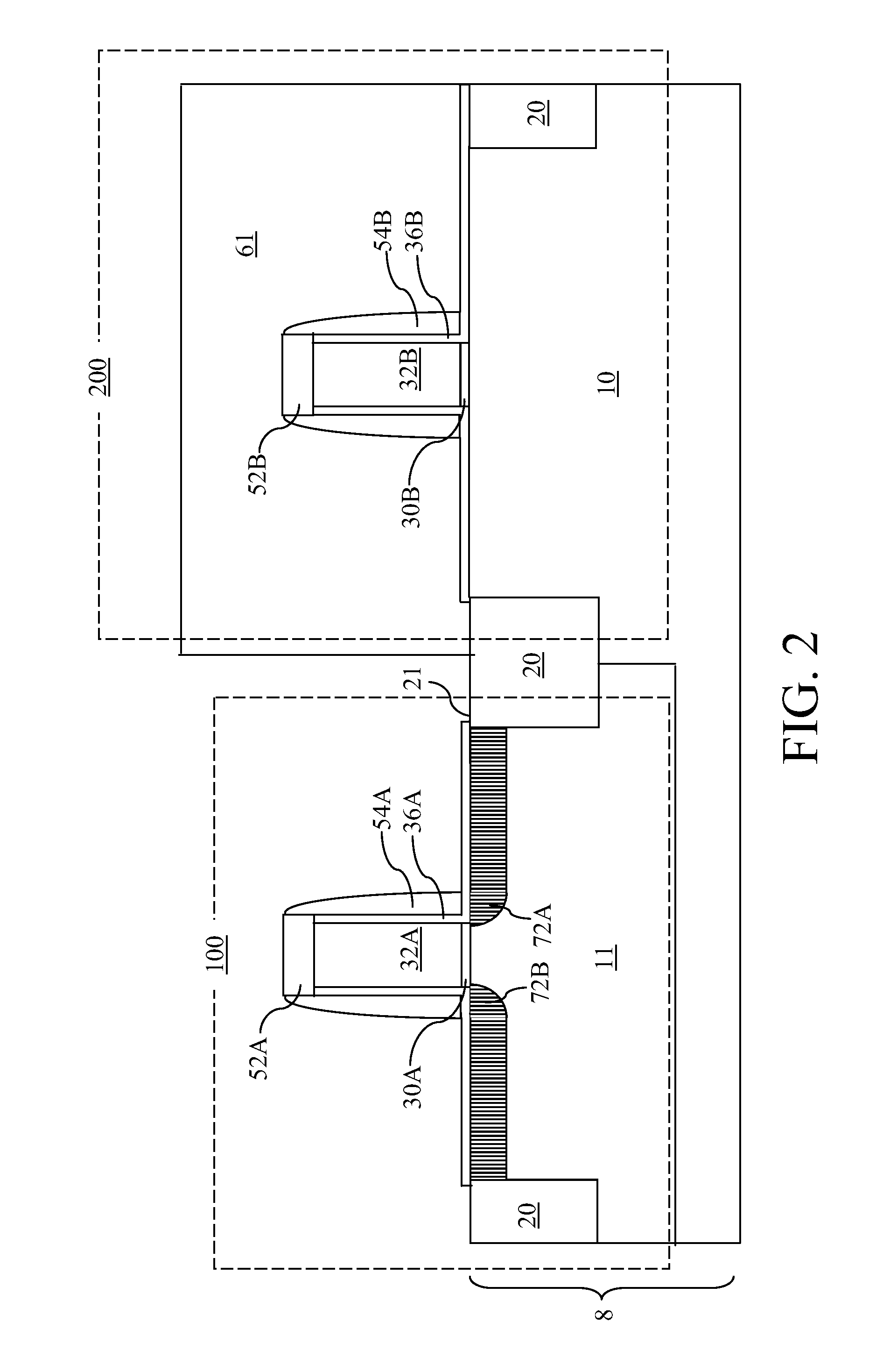
[0029]Referring to FIG. 1, an exemplary semiconductor structure according to a first embodiment of the present disclosure is shown, which includes a semiconductor substrate 8 containing a first semiconductor region 10 and a shallow trench isolation structure 20. The semiconductor substrate 8 can be a bulk substrate including a bulk semiconductor material throughout, or a semiconductor-in-insulator (SOI) substrate (not shown) containing a top semiconductor layer, a buried insulator layer located under the top semiconductor layer, and a bottom semiconductor layer located under the buried insulator layer. The semiconductor material of the semicond...


PUM

PropertyMeasurementUnit
temperatureaaaaaaaaaa
thicknessesaaaaaaaaaa

Abstract

Contact via holes are etched in a dielectric material layer overlying a semiconductor layer to expose the topmost surface of the semiconductor layer. The contact via holes are extended into the semiconductor material layer by continuing to etch the semiconductor layer so that a trench having semiconductor sidewalls is formed in the semiconductor material layer. A metal layer is deposited over the dielectric material layer and the sidewalls and bottom surface of the trench. Upon an anneal at an elevated temperature, a metal semiconductor alloy region is formed, which includes a top metal semiconductor alloy portion that includes a cavity therein and a bottom metal semiconductor alloy portion that underlies the cavity and including a horizontal portion. A metal contact via is formed within the cavity so that the top metal semiconductor alloy portion laterally surrounds a bottom portion of a bottom portion of the metal contact via.

Description

BACKGROUND[0001]The present disclosure relates to metal semiconductor alloy structures for providing low contact resistance and methods of forming the same.[0002]Metal semiconductor alloys such as metal silicides, metal germanides, metal germano-silicides reduce contact resistance between a metal structure such as a metal contact via structure and a semiconductor region such as a source region, a drain region, and a gate conductor line. Formation of metal semiconductor alloys requires an interdiffusion between a metal and a semiconductor material. Typically, the metal is provided as a metal layer, which is deposited after deposition of a dielectric material layer overlying a semiconductor layer and formation of holes within the dielectric material layer to expose the semiconductor material on the top surface of the semiconductor layer. The interface between the metal layer and the underlying semiconductor material is subjected to an anneal at an elevated temperature, typically from ...

Claims


Application Information

Patent Timeline
Patent Type & Authority Applications(United States)
IPC IPC(8): H01L27/088H01L21/336H01L21/8234H01L29/78
CPCH01L21/28518H01L21/76805H01L2924/0002H01L21/76829H01L21/76895H01L21/823807H01L21/823814H01L21/823871H01L29/165H01L29/41766H01L29/665H01L29/6659H01L29/66636H01L29/7834H01L29/7843H01L29/7848H01L2924/00H01L23/485
Inventor HARAN, BALASUBRAMANIAN S.KANAKASABAPATHY, SIVANANDA K.
Owner IBM CORP
Why Eureka
Try Eureka