Light emitting diode package structure

a technology of light-emitting diodes and package structures, which is applied in the direction of semiconductor/solid-state device details, other domestic articles, coatings, etc., can solve the problems of less connection strength, lens disconnection from the substrate easily, and the manufacturing time and cost cannot be reduced, so as to reduce the material cost. the effect of greatly

Inactive Publication Date: 2012-02-16
LIANG MENG PLASTIC SHARE
View PDF2 Cites 17 Cited by
  • Summary
  • Abstract
  • Description
  • Claims
  • Application Information

AI Technical Summary

Benefits of technology

[0010]The present invention has the following advantageous features. The first lens covering

Problems solved by technology

As a result, the manufacturing time and cost cannot be reduced.
However, the lens is formed into a thin shell with a less connecting strength, so that the lens may be disco

Method used


Image

  • Light emitting diode package structure
  • Light emitting diode package structure
  • Light emitting diode package structure

Examples


Embodiment Construction

[0016]The detailed description and technical contents of the present invention will become apparent with the following detailed description accompanied with related drawings. It is noteworthy to point out that the drawings is provided for the illustration purpose only, but not intended for limiting the scope of the present invention.

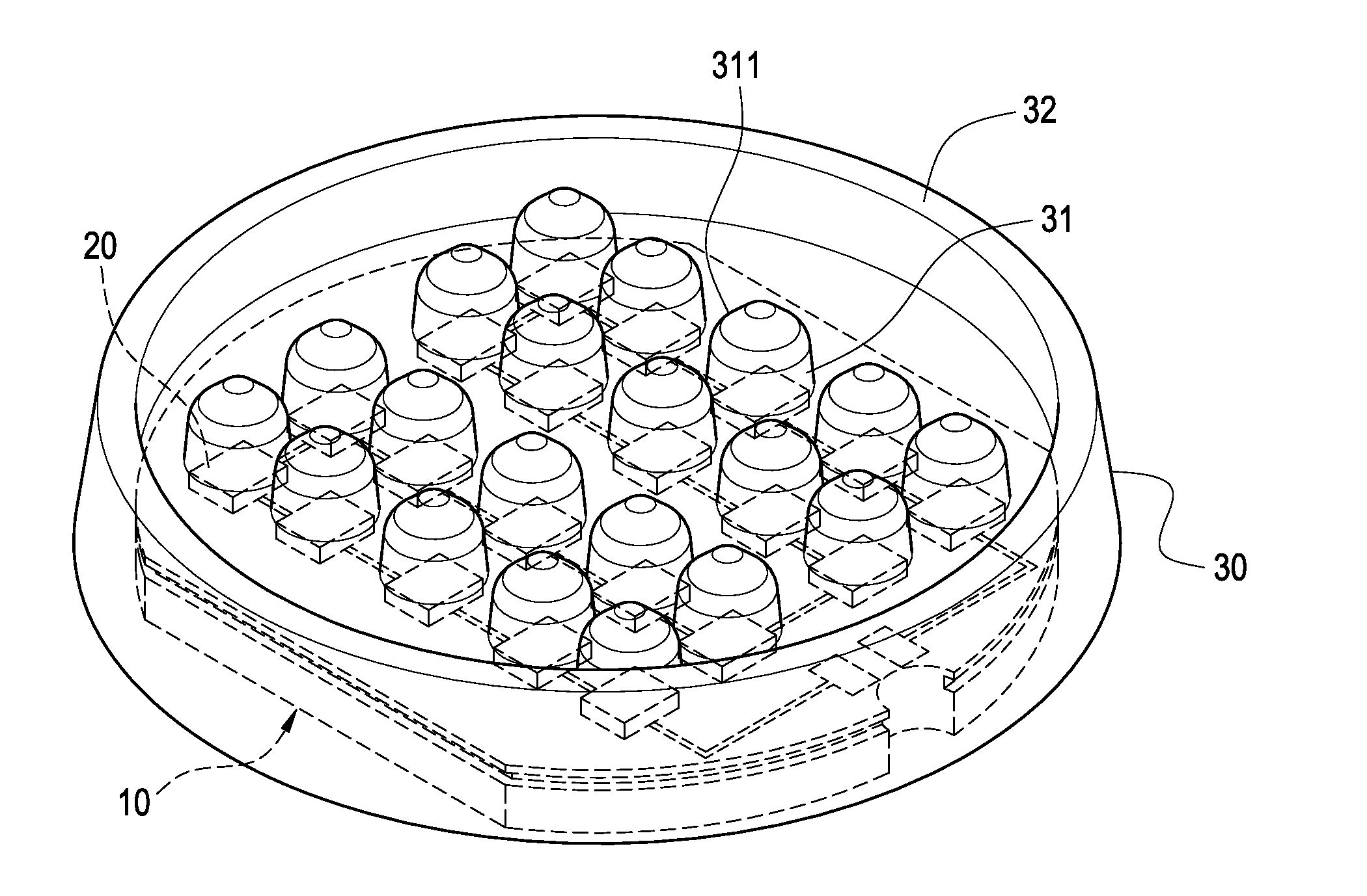
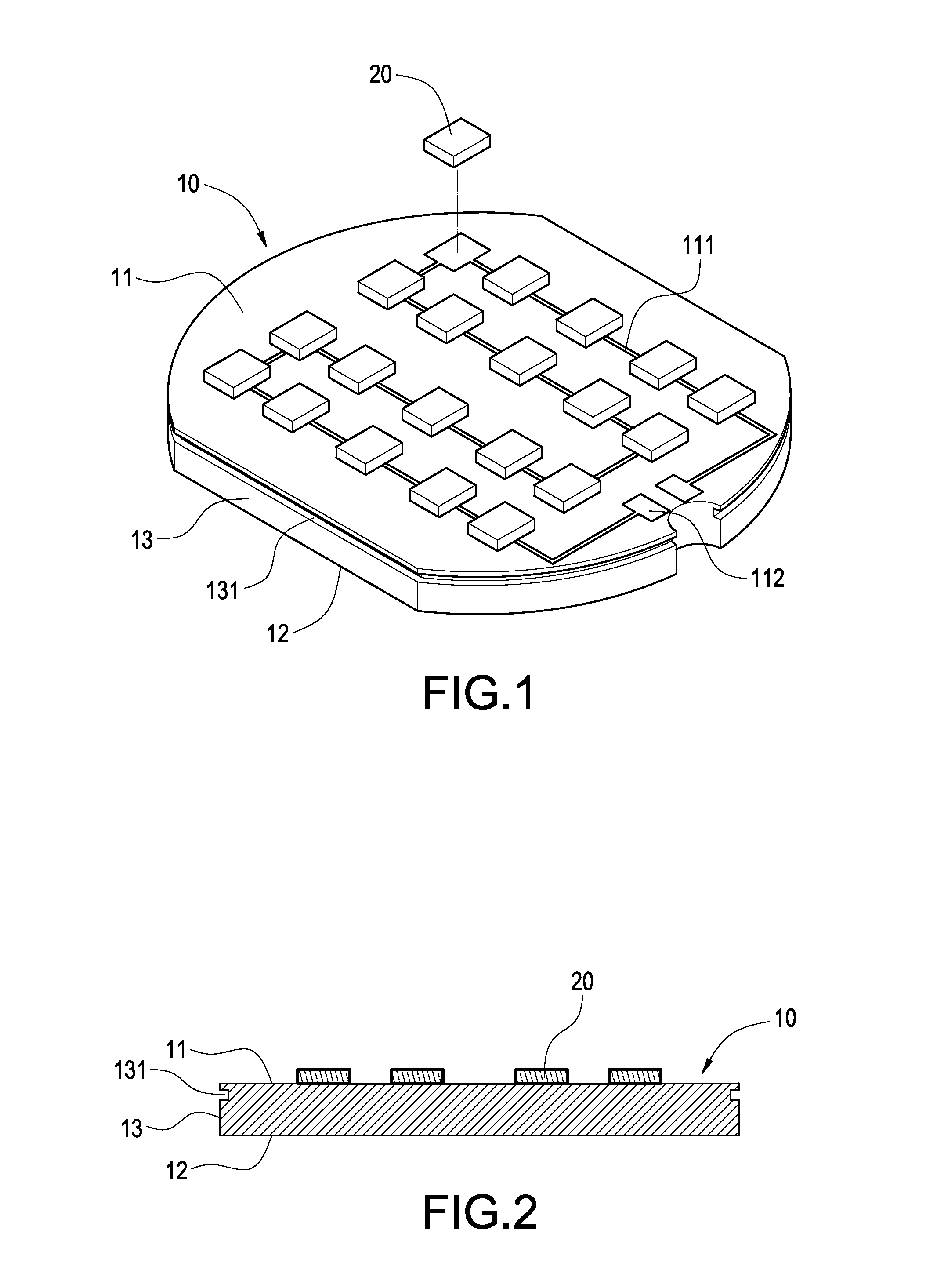
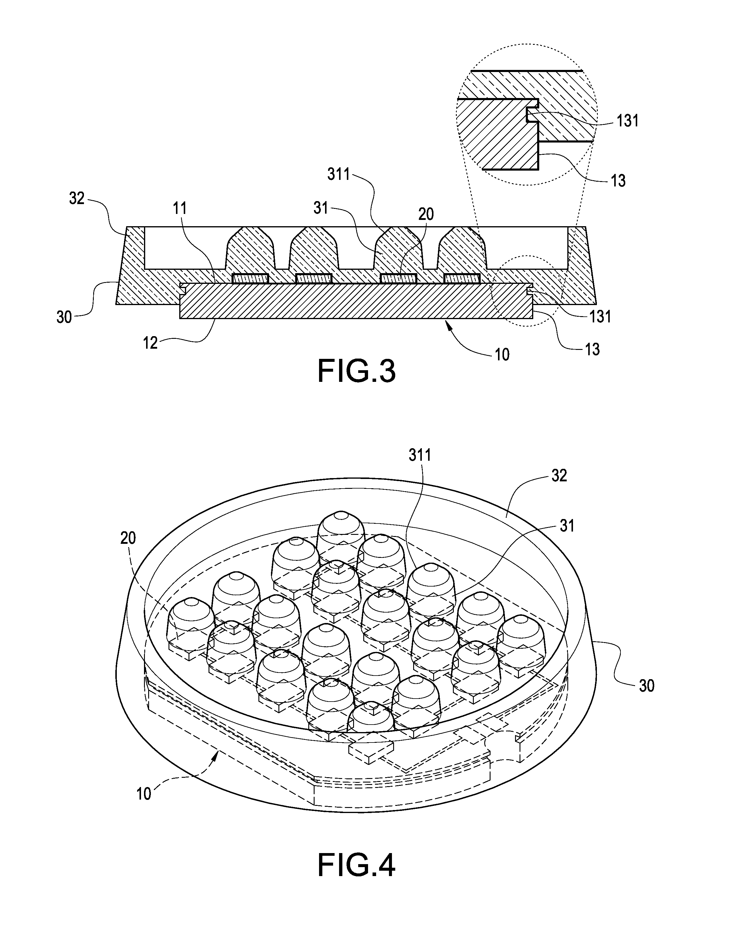
[0017]Please refer to FIGS. 1 and 2. The present invention provides a light emitting diode package structure including a substrate 10, a plurality of LED bare chips 20 and a lens 30.

[0018]The substrate 10 is made of metallic materials having good heat conductivity such as aluminum, copper or alloys thereof. The substrate 10 is formed into a capsule shape and has an upper surface 11, a lower surface 12 and a side surface 13. The lower surface 12 is located below the upper surface 11. The side surface 13 is formed vertically between the upper surface 11 and the lower surface 12. The upper surface 11 is provided with a circuit pattern 111. Copper clad circu...


PUM

PropertyMeasurementUnit
Metallic bondaaaaaaaaaa
aaaaaaaaaa

Abstract

A light emitting diode package structure includes a substrate (10), LED bare chips (20) and a lens (30). The substrate (10) has an upper surface (11), a lower surface (12) and a side surface (13) between the upper surface (11) and the lower surface (12). The upper surface (11) is provided with a circuit pattern (111). The side surface (13) is provided with a groove (131). The LED bare chips (20) are fixed on the upper surface (11) and electrically connected with the circuit pattern (111). The lens (30) covers the LED bare chips (20), the upper surface (11) and the circuit pattern (111) by an injection molding process so as to be inserted into the groove (131). With this arrangement, the connecting strength between the substrate (10) and the lens (30) can be enhanced, thereby achieving waterproof and anti-electrostatic effects. Further, material cost of the present invention is reduced greatly.

Description

BACKGROUND OF THE INVENTION[0001]1. Field of the Invention[0002]The present invention relates to an illumination device, in particular to a light emitting diode package structure.[0003]2. Description of Prior Art[0004]Since light emitting diodes (referred to as “LED” hereinafter) are energy-saving, they have become a new-generation light source for replacing traditional bulbs. Currently, LEDs have been widely used in indoor or outdoor illumination.[0005]A conventional light emitting diode package structure is proposed, in which an upper surface of a substrate is provided with an annular groove. A LED chip is mounted on the surface of substrate on which the annular groove is formed. A binder made of silicon materials is filled into the groove, and then a lens covers outside the LED chip. The bottom of the lens is embedded into the groove and combined therewith.[0006]However, the conventional light emitting diode package structure merely allows one LED chip to be mounted thereon. When...

Claims


Application Information

Patent Timeline
IPC IPC(8): H01L33/58
CPCB29C45/14311B29C45/14655B29L2011/0016H01L25/0753H01L33/54H01L33/58H01L2924/0002H01L2924/00
Inventor LAI, KUANG-CHU
Owner LIANG MENG PLASTIC SHARE
Why Eureka
Try Eureka