Display device having touch panel
a display device and touch technology, applied in the field of display devices having touch panels, can solve the problems of touch screen or display devices easily damaged, touch sensor in touch panels may malfunction, etc., and achieve the effect of intercepting noise generated by display panels and preventing touch panel malfunctions
- Summary
- Abstract
- Description
- Claims
- Application Information
AI Technical Summary
Benefits of technology
Problems solved by technology
Method used
Image
Examples
first embodiment
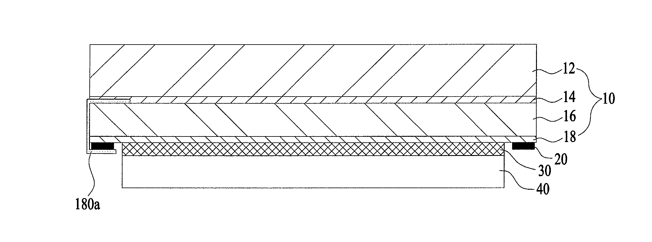
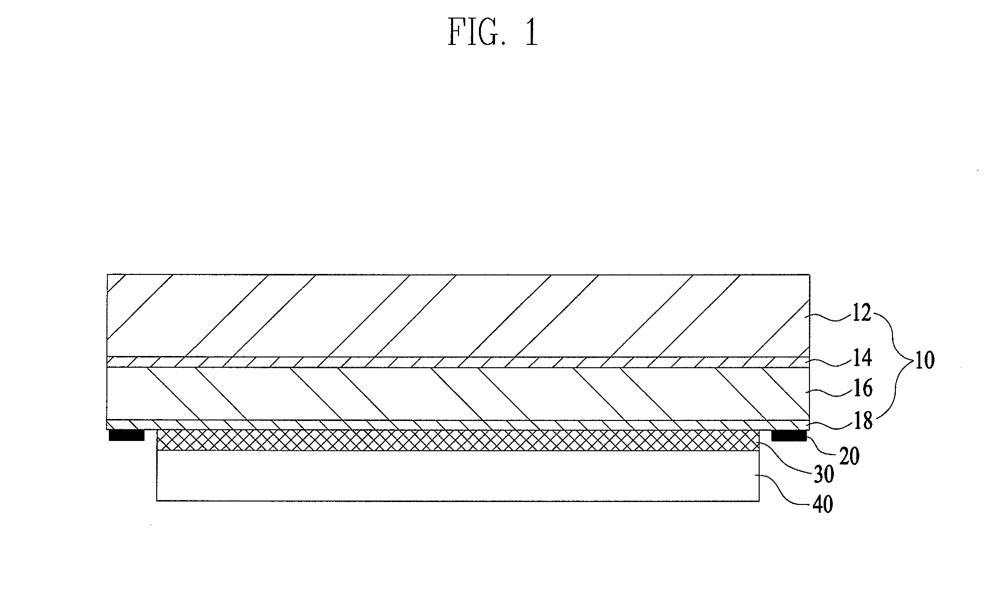
[0029]FIG. 1 is a schematic longitudinal-sectional view of a display device having a touch panel in accordance with a first embodiment of the present invention.
[0030]The display device shown in FIG. 1 includes a display panel 40 and a touch panel 10 attached to the surface of the display panel 40 by an adhesion layer 30.
[0031]As the display panel 40, a flat display device, such as a liquid crystal display device, a plasma display panel or an organic light emitting diode display device, is generally used. For example, if a liquid crystal display device is used as the display panel 40, the liquid crystal display device includes a color filter substrate on which a color filter array is formed, a thin film transistor substrate on which a thin film transistor array is formed, a liquid crystal layer formed between the color filter substrate and the thin film transistor substrate, and polarizing plates respectively attached to the outer surfaces of the color filter substrate and the thin f...
second embodiment
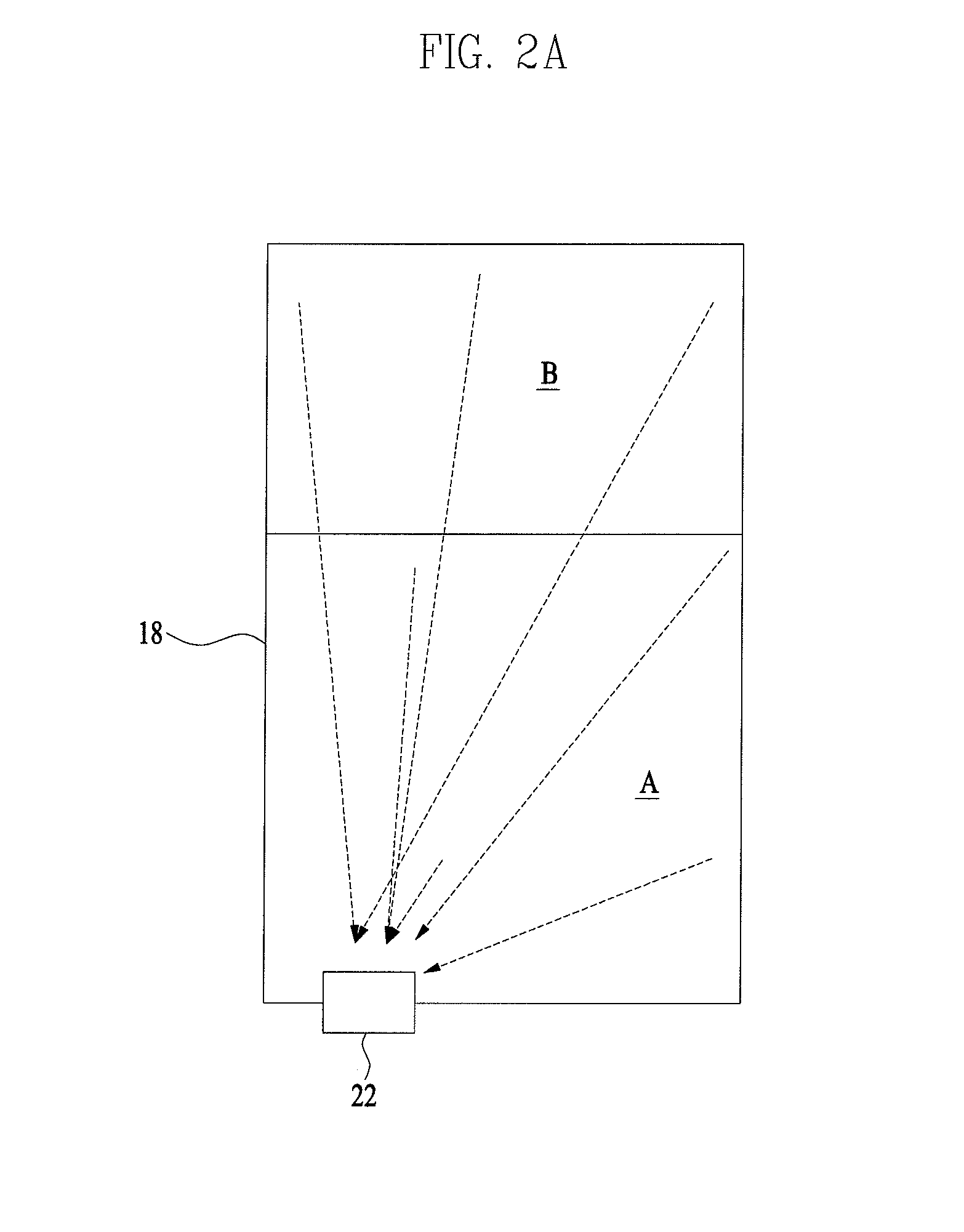
[0045]Even if the metal ring pattern 20 having lower electrical resistance than the transparent conductive layer is formed at the edge of the noise interception layer 18, the central portion of the noise interception layer 18 may have a higher electrical resistance value than the portion of the noise interception layer 18 where the metal ring pattern 20 is formed.
[0046]In order to solve such a problem, the relatively higher electrical resistance value of the central portion of the noise interception layer 18, a metal line cannot be randomly formed at the central portion of the noise interception layer 18. The reason is that the metal line formed at the central portion of the noise interception layer 18 blocks a screen displayed on the display device.
[0047]From among display devices, a liquid crystal display device includes a thin film transistor array substrate, a color filter array substrate and a liquid crystal layer filling a gap between the two substrates.
[0048]The thin film tra...
PUM
 Abstract
Description
Claims
Application Information


