Driving method of semiconductor device

Active Publication Date: 2012-03-15
SEMICON ENERGY LAB CO LTD
View PDF1 Cites 33 Cited by
  • Summary
  • Abstract
  • Description
  • Claims
  • Application Information

AI Technical Summary

Benefits of technology

[0036]The driving method of a semiconductor device according to one embodiment of the disclosed invention can be realized by using the above-described semiconductor device in which a transistor including a material other than an oxide semiconductor and a transistor including an oxide semiconductor are combined. When writing is performed on a memory cell of the semiconductor device, a first transistor including a material other than an oxide semico

Problems solved by technology

The reliability of a storage device is decreased by

Method used


Image

  • Driving method of semiconductor device
  • Driving method of semiconductor device
  • Driving method of semiconductor device

Examples


Example

Embodiment 1

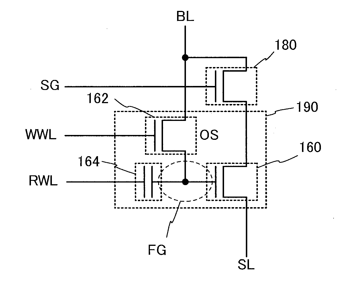
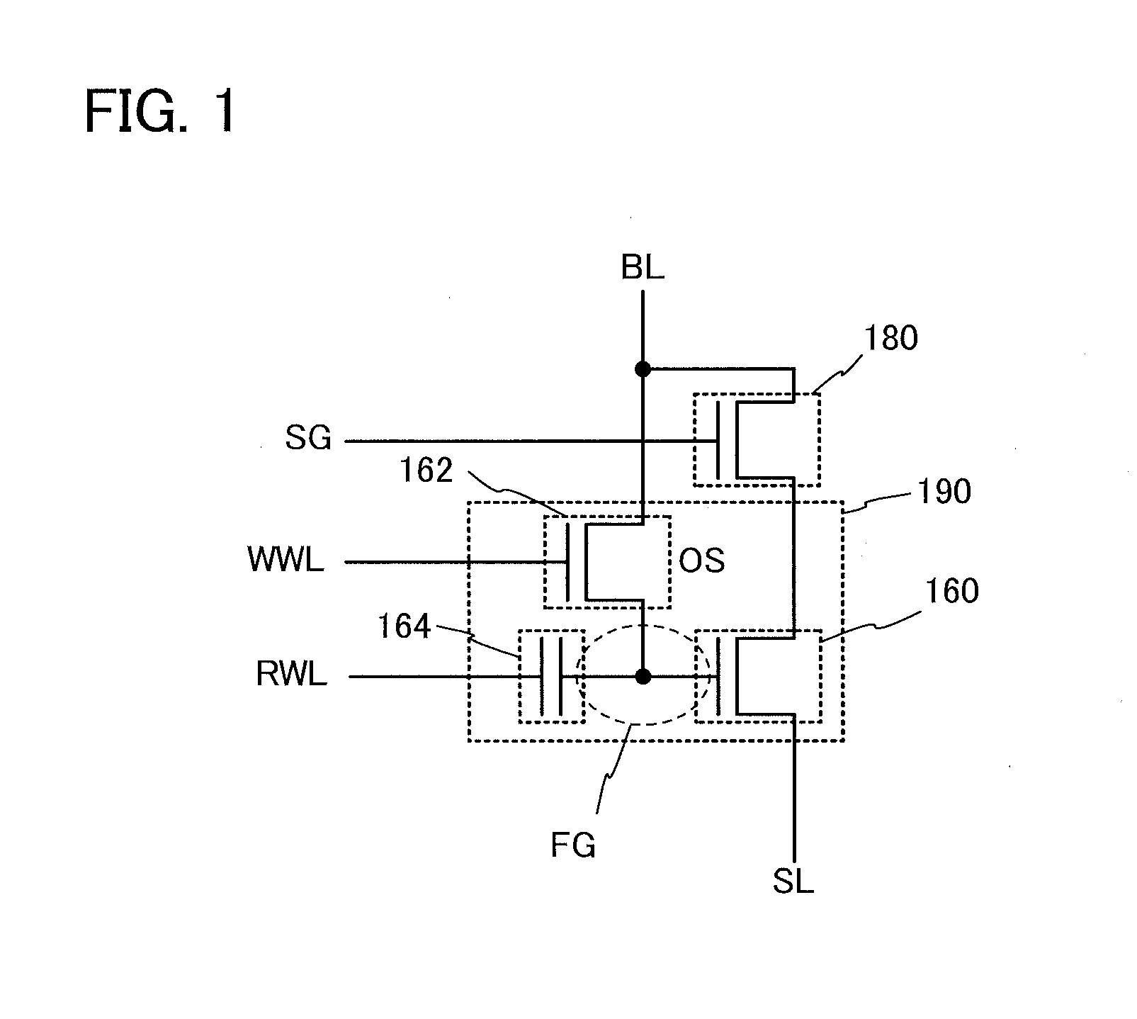
[0071]In this embodiment, a circuit configuration and operation of a semiconductor device according to one embodiment of the invention disclosed herein will be described with reference to FIG. 1. Note that in a circuit diagram, in some cases, “OS” is written beside a transistor in order to indicate that the transistor includes an oxide semiconductor material.

[0072]First, a basic circuit configuration and circuit operation will be described with reference to FIG. 1. In the circuit diagram in FIG. 1, one of a source electrode and a drain electrode (e.g., the drain electrode) of a selection transistor 180, one of a source electrode and a drain electrode (e.g., the drain electrode) of a transistor 162, and a bit line BL are electrically connected to one another. The other of the source electrode and the drain electrode (e.g., the source electrode) of the selection transistor 180 is electrically connected to one of a source electrode and a drain electrode (e.g., the drain ele...

Example

Embodiment 2

[0144]In this embodiment, a circuit configuration and operation of a semiconductor device according to one embodiment of the invention disclosed herein will be described with reference to FIG. 4. Note that in a circuit diagram, “OS” is written beside a transistor in order to indicate that the transistor includes an oxide semiconductor material.

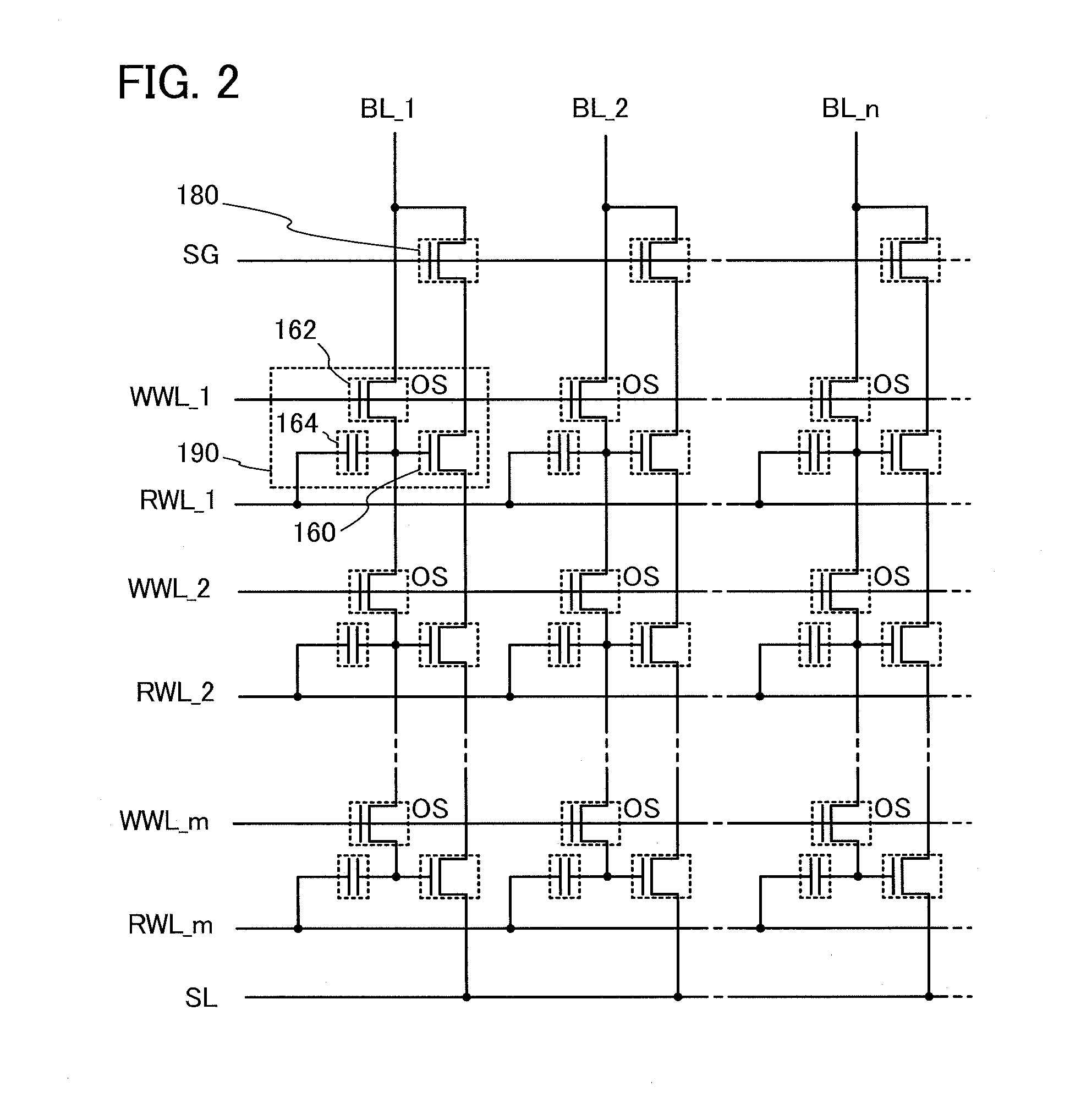
[0145]The circuit configuration shown in FIG. 4 is an example of a circuit configuration of a NAND-type semiconductor device including r (in a vertical direction)×n (in a horizontal direction) blocks 700 (r is a natural number greater than or equal to 1), in which one block includes in memory cells 190 and a selection transistor 180. The configuration of the block 700 in FIG. 4 is similar to the configuration in FIG. 2. Note that either the source electrodes or drain electrodes of the selection transistors 180 in each of the r blocks 700 electrically connected in the vertical direction are electrically connected to the same bit lin...

Example

Embodiment 3

[0154]In this embodiment, a structure and a manufacturing method of a semiconductor device according to one embodiment of the invention disclosed herein will be described with reference to FIGS. 5A and 5B, FIGS. 6A to 6G, FIGS. 7A to 7E, FIGS. 8A to 8D, FIGS. 9A to 9D, FIGS. 10A to 10C, FIGS. 11A to 11C, and FIGS. 12A and 12B. Specifically, a structure and a manufacturing method of a memory cell which can be mounted on a storage device will be described.

[0155]FIGS. 5A and 5B illustrate an example of a structure of a semiconductor device. FIG. 5A illustrates a cross section of the semiconductor device, and FIG. 5B illustrates a plan view of the semiconductor device. Here, FIG. 5A corresponds to a cross section along line A1-A2 and line B1-B2 in FIG. 5B. The semiconductor device illustrated in FIGS. 5A and 5B includes the transistor 160 including a first semiconductor material in a lower portion and the transistor 162 including a second semiconductor material in an upper p...


PUM


Abstract

A driving method of a semiconductor device is provided. In a semiconductor device including a bit line, a selection line, a selection transistor, m (m is a natural number greater than or equal to 2) writing word lines, m reading word lines, a source line, and first to m-th memory cells, each memory cell includes a first transistor and a second transistor that holds charge accumulated in a capacitor. The second transistor includes a channel formed in an oxide semiconductor layer. In a driving method of a semiconductor device having the above structure, when writing to a memory cell is performed, the first transistor is turned on so that a first source terminal or a first drain terminal is set to a fixed potential; thus, a potential is stably written to the capacitor.

Description

BACKGROUND OF THE INVENTION[0001]1. Field of the Invention[0002]The invention disclosed herein relates to a semiconductor device using a semiconductor element and a method for driving the semiconductor device.[0003]2. Description of the Related Art[0004]Storage devices using semiconductor elements are broadly classified into two categories: a volatile device that loses stored data when power supply stops, and a non-volatile device that holds stored data even when power is not supplied.[0005]A typical example of a volatile storage device is a DRAM (dynamic random access memory). A DRAM stores data in such a manner that a transistor included in a storage element is selected and charge is accumulated in a capacitor.[0006]When data is read from a DRAM, charge in a capacitor is lost on the above-described principle; thus, another writing operation is necessary whenever data is read out. Moreover, since leakage current (off-state current) flows between a source and a drain of a transistor...

Claims


Application Information

Patent Timeline
IPC IPC(8): G11C11/24
CPCG11C11/404G11C11/403H01L27/1214
Inventor MATSUZAKI, TAKANORIKATO, KIYOSHI
Owner SEMICON ENERGY LAB CO LTD
Why Eureka
Try Eureka