Receiver chip and method for on-chip multi-node visible light communication

a multi-node visible light and receiver chip technology, applied in the field of optical communication, can solve the problems of difficult application of transmissions to mobile receivers (or from mobile transmitters), limited possibilities for narrow angle transmission or reception, and similar disadvantages of both methods in wide angle transmissions

Active Publication Date: 2012-03-29
SUPREME ARCHITECTURE
View PDF2 Cites 64 Cited by
  • Summary
  • Abstract
  • Description
  • Claims
  • Application Information

AI Technical Summary

Benefits of technology

[0013]A system for on-chip multi-node visible light communication according to some embodiments of the present invention may include: an array of receiver cells including an array of photodetectors, each receiver cell includes at least one photodetector and is to receive light thro

Problems solved by technology

Although the optical communication is much more efficient than RF communication, both methods have a similar disadvantage in wide angle transmissions.
However, the possibilities in using narrow angle transmission or reception are very limited due to the directionality of the transmission.
The narrow angle requires accurate detection and aiming of the transmission to the receiver, and th

Method used


Image

  • Receiver chip and method for on-chip multi-node visible light communication
  • Receiver chip and method for on-chip multi-node visible light communication
  • Receiver chip and method for on-chip multi-node visible light communication

Examples


Embodiment Construction

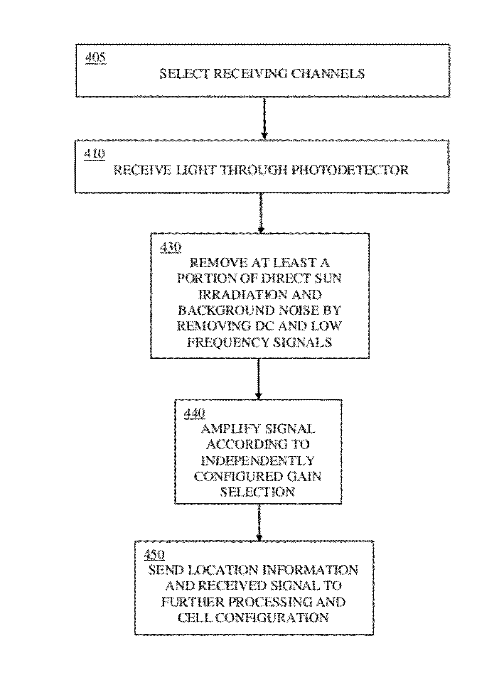
[0029]In the following detailed description, numerous specific details are set forth in order to provide a thorough understanding of the invention. However, it will be understood by those skilled in the art that the present invention may be practiced without these specific details. In other instances, well-known methods, procedures, and components have not been described in detail so as not to obscure the present invention.

[0030]Embodiments of the present invention may provide a receiver chip and method for improved optical wireless communication. An optical receiver chip provided by embodiments of the present invention may support mobile communication for multiple independent and fast channels simultaneously, and thus may enable new applications. Additionally, an optical receiver chip provided by embodiments of the present invention may be compact in size.

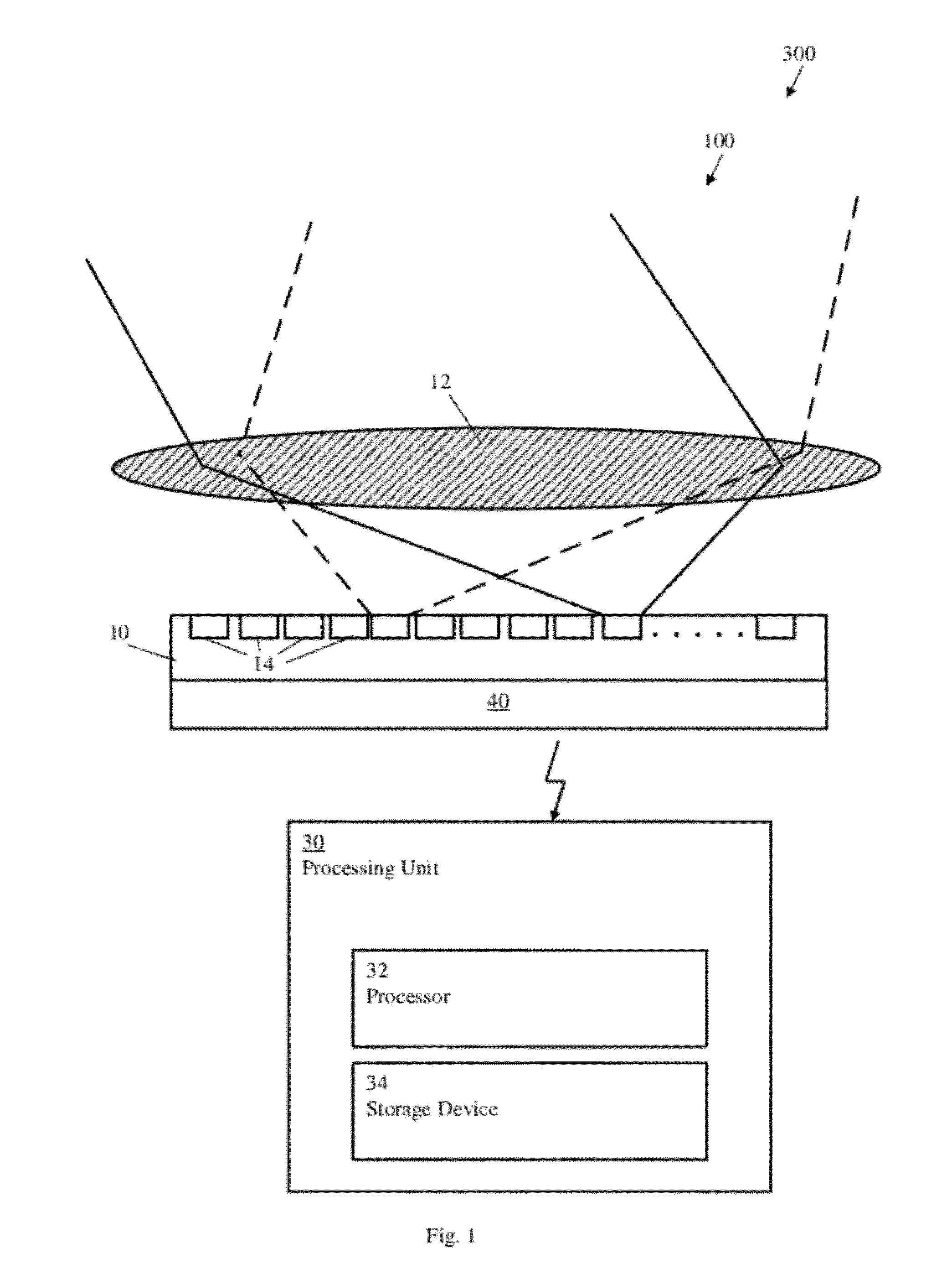
[0031]Reference is now made to FIG. 1, which is a schematic illustration of a system 300 for on-chip multi-node visible light co...


PUM


Abstract

A receiver chip, system and method for on-chip multi-node visible light communication, the receiver chip comprising: an array of receiver cells comprising an array of photodetectors, each receiver cell comprises at least one photodetector and is to receive light through the at least one photodetector, and a logical layer for independently configuring at least one selected receiver cell as a communication receiving channel. The system comprises an array of receiver cells comprising an array of photodetectors, each receiver cell includes at least one photodetector and is to receive light through the at least one photodetector, a logical layer to independently configure at least one selected receiver cell as a communication receiving channel, and a processor to receive data from the logical layer and control the logical layer for configuration of the receiver cells.

Description

CROSS REFERENCE TO RELATED APPLICATIONS[0001]This application claims the benefit of U.S. Provisional Application Ser. No. 61 / 387,506, filed Sep. 29, 2010, which is hereby incorporated by reference in its entirety.BACKGROUND OF THE INVENTION[0002]In the field of optical communication which does not use optical guides / fibers in order to transmit the communication, several methods are known. These methods belong to several different sub-classes, usually referred to by different terms, such as Wireless / Fiberless Optical Communication (WOC / FOC, mainly used to describe indoors, short range systems), Free Space Optical Communication (FSO, mainly used to describe outdoors, mid / long range systems), Visible Light Communication (VLC, mainly used to describe indoors and outdoors, on the visible light spectrum).[0003]It is estimated that for the same conditions of data rate, power, distances, angles, etc. optical communication is about ten times more efficient than RF communication. Usually, the...

Claims


Application Information

Patent Timeline
IPC IPC(8): H04B10/06
CPCH04B10/60H04B10/116
Inventor GUROVICH, MARTINSHWARTZ, JOSEF
Owner SUPREME ARCHITECTURE
Why Eureka
Try Eureka