Condenser microphone array chip

a technology of condenser microphones and array chips, applied in the field of micro electromechanical systems, can solve the problems of warpage of the chip, easy warpage or bent of the chip area including the array of condenser microphones during manufacturing processes, etc., to simplify the overall structure of the condenser microphone array chip, reduce manufacturing costs, and reduce chip warpage.

Active Publication Date: 2012-04-05
INFINEON TECH AG
View PDF4 Cites 32 Cited by
  • Summary
  • Abstract
  • Description
  • Claims
  • Application Information

AI Technical Summary

Benefits of technology

[0014]It is an object of the present invention to provide a condenser microphone array chip including a plurality of MEMS condenser microphones with reduced warpage of a substrate.

Problems solved by technology

An area of a chip including an array of condenser microphones are easily warped or bent during manufacturing processes.
The manufacturing processes of condenser microphone array chips do include annealing in order to alleviate stress applied to the first electrode layer or the second electrode layer (which is used to make vibrating electrodes), whereas annealing adversely functions to increase stress applied to the first insulating layer or the second insulating layer, which may result in warpage of a chip.

Method used


Image

  • Condenser microphone array chip
  • Condenser microphone array chip
  • Condenser microphone array chip

Examples


Embodiment Construction

[0049]The present invention will be described in further detail by way of examples with reference to the accompanying drawings.

1. Constitution

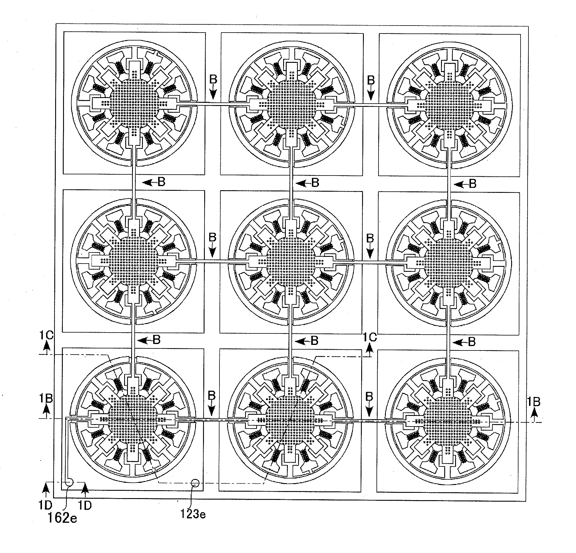
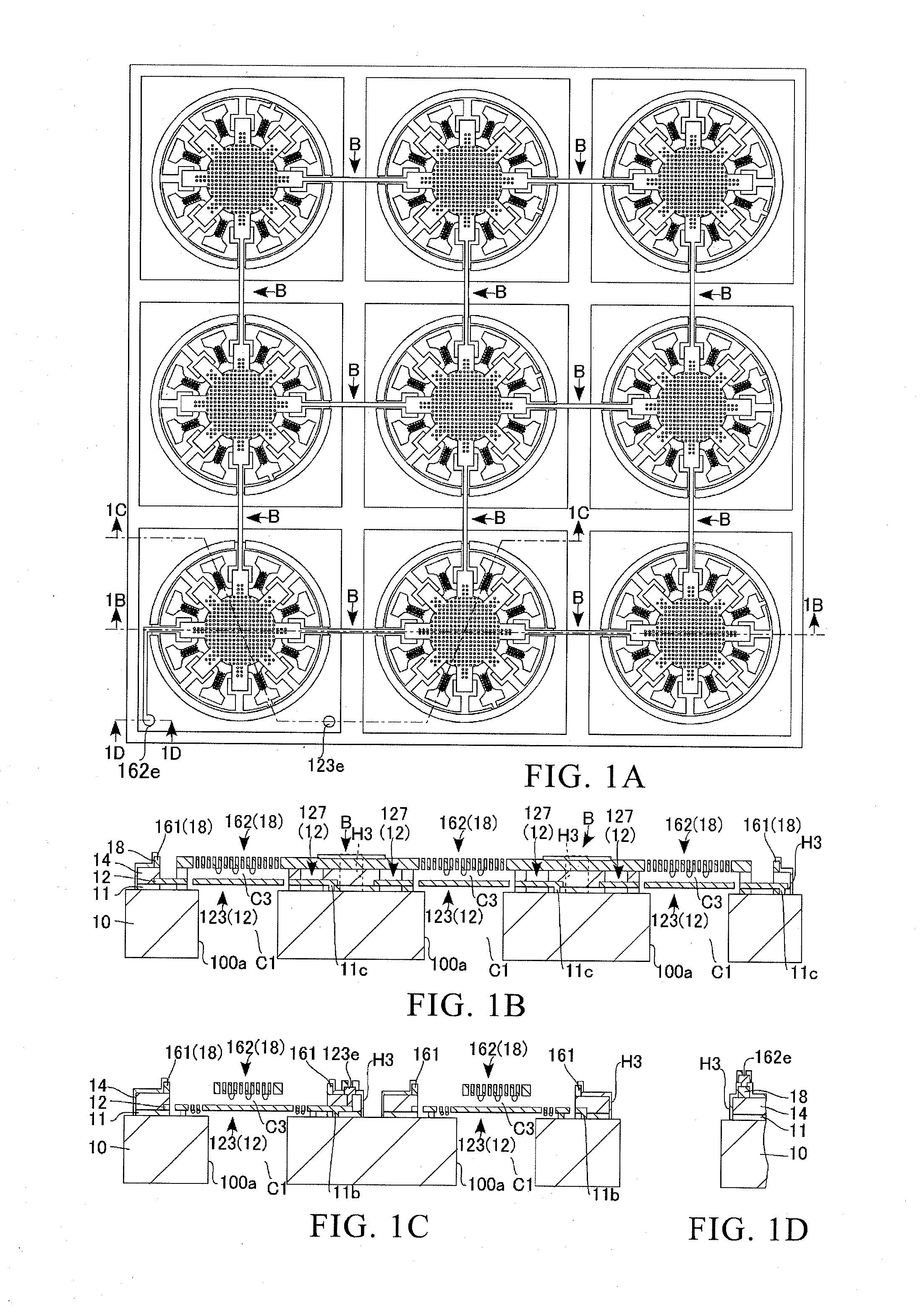
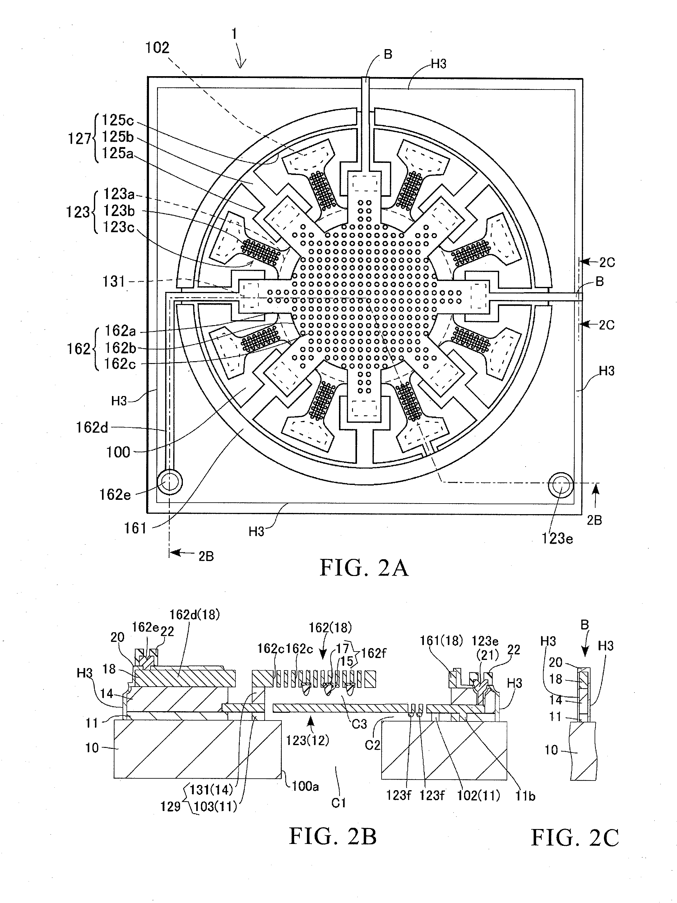
[0050]FIGS. 1A, 1B, 1C, 1D show a condenser microphone array chip according to a preferred embodiment of the present invention. FIG. 1A is a plan view of the condenser microphone array chip; FIG. 1B is a cross-sectional view taken along line 1B-1B in FIG. 1A; FIG. 1C is a traverse sectional view taken along line 1C-1C in FIG. 1A; and FIG. 1D is a partial sectional view taken along line 1D-1D in FIG. 1A. In the condenser microphone array chip, nine structures are formed on a substrate 10. FIG. 2A is a plan view of a single structure of a condenser microphone; FIG. 2B is a traverse sectional view taken along line 2B-2B in FIG. 2A; and FIG. 2C is a partial sectional view taken along line 2C-2C in FIG. 2A. FIG. 3 is an exploded perspective view showing layers constituting a single structure. For the sake of simplification of illustration, a surfac...


PUM


Abstract

A plurality of structures of condenser microphones is fabricated in a single condenser microphone array chip. The condenser microphone array chip includes a substrate having a plurality of openings serving as air cavities, a first insulating layer formed in the outer periphery of the openings, a first electrode layer stretched over each of the openings, a second insulating layer formed above the first electrode layer in the outer periphery of the openings, a second electrode layer formed above the second insulating layer relative to the first electrode layer via an air gap therebetween. The structures are connected via a plurality of bridges and separated via a plurality of channels therebetween. The channels circumvent the bridges so that at least the second insulating layer is partially removed from the channels. The bridges are formed using the second electrode layer serving as wiring for electrically connecting the structures of condenser microphones.

Description

BACKGROUND OF THE INVENTION[0001]1. Field of the Invention[0002]The present invention relates to MEMS (Micro Electro-Mechanical System) transducer array chips, and in particular to condenser microphone array chips fabricated with arrays of MEMS condenser microphones.[0003]The present application claims priority on Japanese Patent Application No. 2010-220575, the entire content of which is incorporated herein by reference.[0004]2. Description of the Related Art[0005]It is conventionally known that a single microphone may include a plurality of MEMS condenser microphones. Patent Documents 1-3 disclose microphones in which a plurality of condenser microphones is formed on a single chip. Additionally, it is conventionally known that an S / N ratio can be improved using a plurality of condenser microphones connected in a parallel manner or in a cascaded manner.[0006]A single substrate fabricated with a microphone array including a plurality of MEMS condenser microphones suffers from a prob...

Claims


Application Information

Patent Timeline
Patent Type & Authority Applications(United States)
IPC IPC(8): H04R1/00
CPCB81B2201/0257B81C1/00666H04R7/26H04R2201/401H04R31/00H04R2201/003H04R19/005
Inventor SAKURAUCHI, KAZUSHISUZUKI, TAMITOSUZUKI, YUKITOSHI
Owner INFINEON TECH AG
Why Eureka
Try Eureka