Method for manufacturing semiconductor structure

Active Publication Date: 2012-04-05
INST OF MICROELECTRONICS CHINESE ACAD OF SCI
View PDF24 Cites 2 Cited by
  • Summary
  • Abstract
  • Description
  • Claims
  • Application Information

AI Technical Summary

Benefits of technology

[0008]It is an object of the present invention to provide SMT for a pFET, which may be used to apply compressive stress to a channel of the pFET with conventional stress-inducing materials, and which may memorize the compressive stress from the stress-in

Problems solved by technology

One of the problems with the SMT is that it may only be applied to nFETs.
However, those materials used for applying the stress to the field effect

Method used


Image

  • Method for manufacturing semiconductor structure
  • Method for manufacturing semiconductor structure
  • Method for manufacturing semiconductor structure

Examples


Example

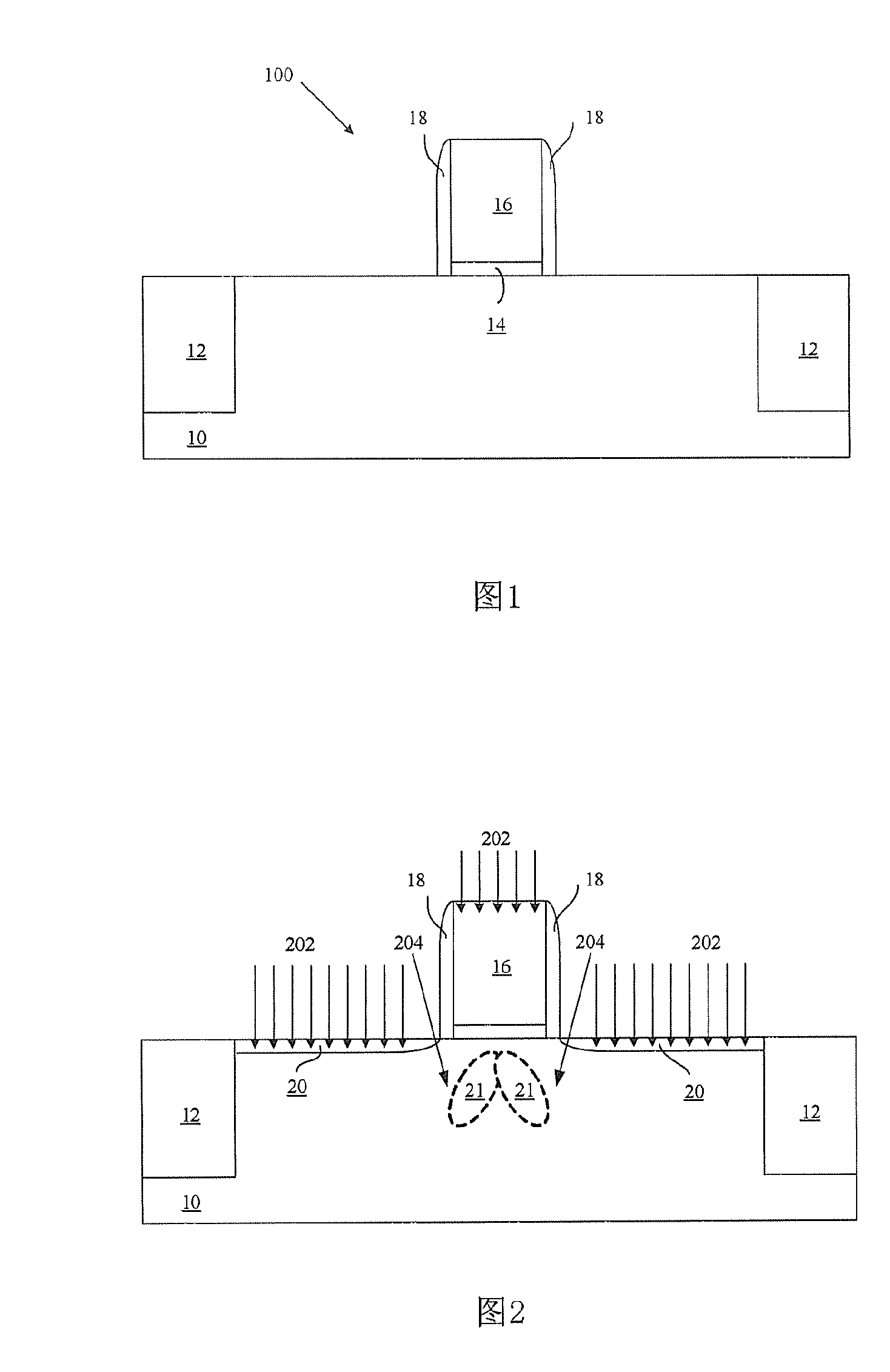
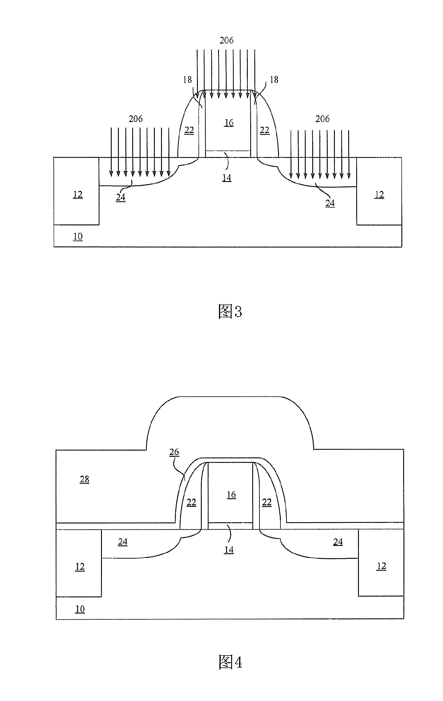
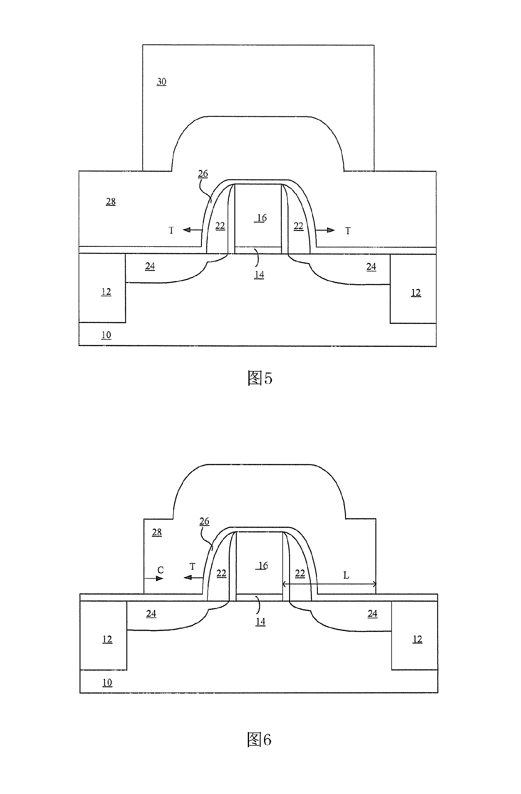
[0025]The present invention will be described below with preferred embodiments in connection with attached drawings. However, it should be understood that the descriptions here are only illustrative and are not intended to limit the protection scope. Also, the following description omits details of known structures and techniques so that concepts of the invention are not obscured unnecessarily.

[0026]Top views, cross-sectional views and perspective views of various structures of the semiconductor structure according to the embodiments of the present invention are shown in attached drawings. However, these figures are not drawn to scale, and some details may be exaggerated and other details may be omitted for simplicity. Shapes, relative sizes and positions of various regions / layers shown in the figures are only illustrative. Variations may exist due to manufacturing tolerance and technical limitations. Moreover, those skilled in the art may design regions / layers having different shap...


PUM


Abstract

The present application discloses a method for manufacturing a semiconductor structure, comprising the steps of: a) providing a p-type field effect transistor; b) forming a tensile-stressed layer on the p-type field effect transistor; c) removing a portion of the tensile-stressed layer, so that the remaining portion of the tensile-stressed layer generates compressive stress in the channel of the p-type field effect transistor; and d) performing annealing, so as to achieve the object of memorizing compressive stress in a channel of a transistor and improving the performance of the transistor. The method according to the present invention memorizes the compressive stress in the channel of the transistor by a stress memorization technique, increases mobility of holes, and improves overall performance of the semiconductor structure.

Description

BACKGROUND OF THE INVENTION[0001]1. Field of Invention[0002]The present invention generally relates to a method for manufacturing a semiconductor structure, and more particularly, to a method for manufacturing a high-performance semiconductor structure by a stress memory technique.[0003]2. Description of Related Art[0004]It is well known that performance of a field effect transistor (FET) may be improved when stress is applied thereto. In such a case that stress is applied to a field effect transistor, tensile stress may increase mobility of electrons, and thus driving current of an nFET, while compressive stress may increase mobility of holes, and thus driving current of a pFET.[0005]One approach for providing such stress is referred to as Stress Memorization Technique (SMT), which comprises forming a material having intrinsic stress, such as silicon nitride, at various locations of a semiconductor structure, for example, above a channel region; performing annealing so that the str...

Claims


Application Information

Patent Timeline
IPC IPC(8): H01L21/28
CPCH01L29/665H01L29/66537H01L29/7847H01L29/6659H01L29/7833H01L29/66545
Inventor ZHU, HUILONG
Owner INST OF MICROELECTRONICS CHINESE ACAD OF SCI
Why Eureka
Try Eureka