Check patentability & draft patents in minutes with Patsnap Eureka AI!

Methods and Systems for Debugging Equivalent Designs Described at Different Design Levels

a technology of equivalent designs and design levels, applied in the field of methods and systems for synchronous debugging of integrated circuit designs, can solve the problems of becoming a technology bottleneck, designers still need to spend a significant amount of time in gate-level implementations,

Active Publication Date: 2012-04-05
SYNOPSYS INC +1
View PDF4 Cites 0 Cited by
  • Summary
  • Abstract
  • Description
  • Claims
  • Application Information

AI Technical Summary

Problems solved by technology

Although automated tools for translating designs at different design levels are provided, designers still need to spend a significant amount of time in gate-level implementations since some design issues can only be discovered and resolved at the gate level.
For example, these design issues may include manual design changes, timing optimizations, post-synthesis debugging, and others.
Due to these design issues, debugging and tracing signals between two different design levels have become a technological bottleneck in the chip design industry.

Method used


Image

  • Methods and Systems for Debugging Equivalent Designs Described at Different Design Levels
  • Methods and Systems for Debugging Equivalent Designs Described at Different Design Levels
  • Methods and Systems for Debugging Equivalent Designs Described at Different Design Levels

Examples


Embodiment Construction

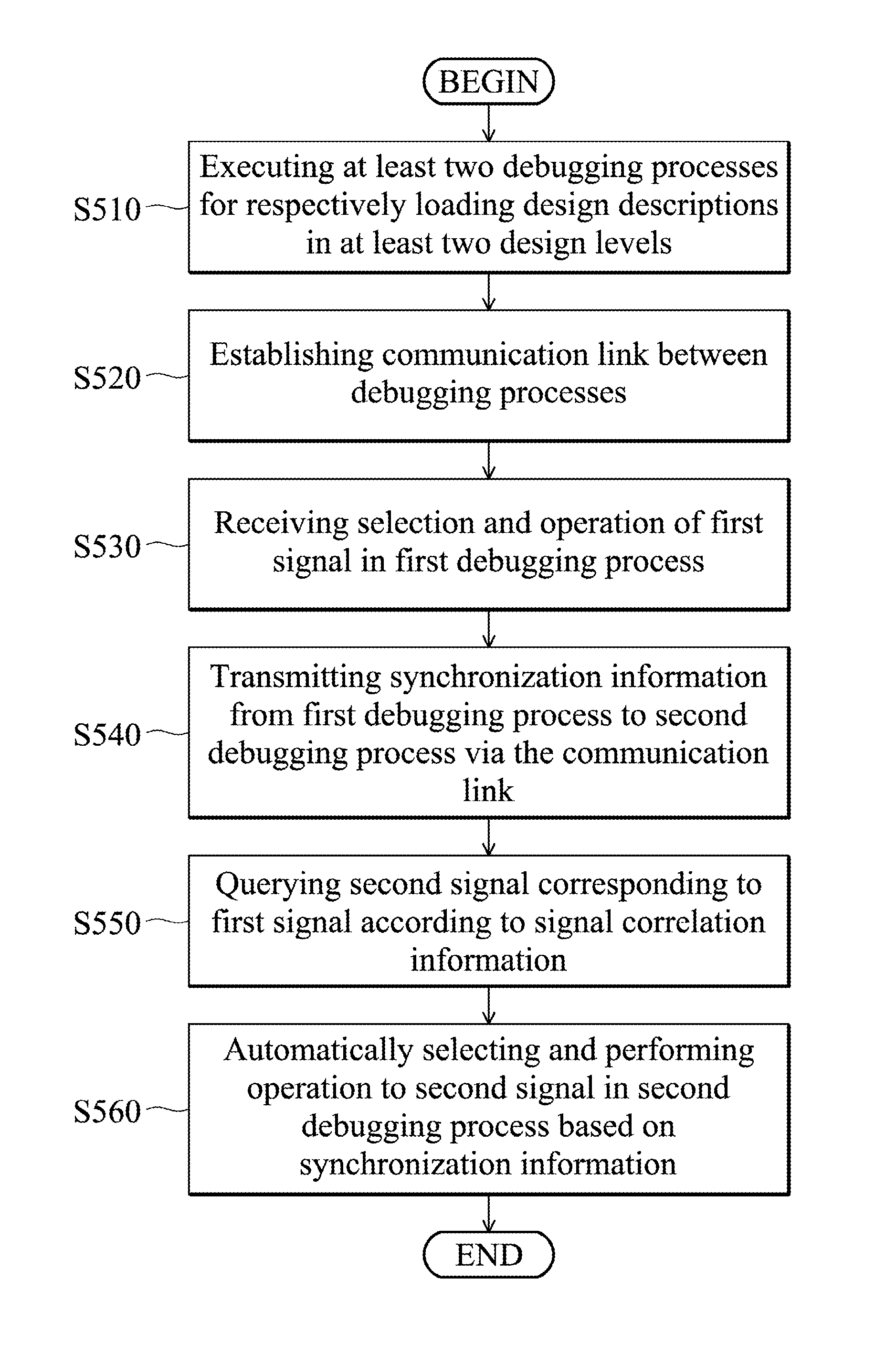
[0022]Methods and systems for debugging designs described equivalently in at least two design levels are provided.

[0023]FIG. 1 is a schematic diagram illustrating an embodiment of a system for debugging designs according to the invention. The system for debugging designs 100 may be a processor-based electronic device, such as a computer system, a workstation, a notebook, or others.

[0024]The system for debugging designs 100 comprises a display unit 110, a storage unit 120, and a processing unit 130. The display unit 110 can display related texts, figures, user interfaces, and other data provided by an operating system and / or applications executed on the system. The storage unit 120 can comprise design descriptions corresponding to a same design at various design levels. For example, the storage unit 120 may comprise an RTL design description 121 and a gate level design description 122. It is noted that the RTL design description 121 and the gate level design description 122 are descr...


PUM


Abstract

Methods for debugging designs are provided. First, signal correlation information for signals of a design at least two design level is obtained. Then, design descriptions corresponding to the design at the at least two design levels are loaded and presented in at least two sets of windows or at least two debugging processes which controls the respective set of windows. A selection of a first signal in a first set of windows or a first debugging process is received. In response to the selection, a second signal corresponding to the first signal is queried according to the signal correlation information, and the second signal in a second set of windows or a second debugging process is automatically selected.

Description

CROSS REFERENCE TO RELATED APPLICATIONS[0001]This application claims the benefit of U.S. Provisional Application No. 61 / 390,047 filed Oct. 5, 2010, the entirety of which is incorporated by reference herein.BACKGROUND OF THE INVENTION[0002]1. Field of the Invention[0003]The disclosure relates generally to methods and systems for debugging designs, and, more particularly to methods and systems for synchronously debugging designs of integrated circuits (ICs) described equivalently at different design levels, such as a register transfer level (RTL) and a gate level.[0004]2. Description of the Related Art[0005]Currently, IC designers mainly work at the RTL when designing complex digital systems, and then synthesize their designs into gate-level implementations with synthesizing tools. Although automated tools for translating designs at different design levels are provided, designers still need to spend a significant amount of time in gate-level implementations since some design issues ca...

Claims


Application Information

Patent Timeline
IPC IPC(8): G06F17/50
CPCG06F17/5022
Inventor KO, LU-ANCHEN, XISHER, ARNOLDTSAI, FURSHING
Owner SYNOPSYS INC
Features
  • R&D
  • Intellectual Property
  • Life Sciences
  • Materials
  • Tech Scout
  • Unparalleled Data Quality
  • Higher Quality Content
  • 60% Fewer Hallucinations
Learn More