Impedance stabilization device
a technology of impedance stabilization and stabilizer, which is applied in waveguide type devices, power distribution line transmission, digital transmission, etc., can solve the problems of channel characteristic degradation in power line communication, impedance mismatch to a line, and power distribution system that is normally not designed for communication use, etc., and achieve the effect of reducing the impedance mismatch
- Summary
- Abstract
- Description
- Claims
- Application Information
AI Technical Summary
Benefits of technology
Problems solved by technology
Method used
Image
Examples
embodiment 1
Modification of Embodiment 1
[0115]The following describes other configurations than those described in Embodiment 1 (see FIGS. 1 and 5) that the impedance stabilization device can have. Note that, for each impedance stabilization device, differences from the impedance stabilization device 1 are mainly described here.
[0116]FIGS. 7A, 7B and 8 each illustrate examples of a configuration that the impedance stabilization device can have.
[0117]First, description is made on an impedance stabilization device 70 illustrated in FIG. 7A.
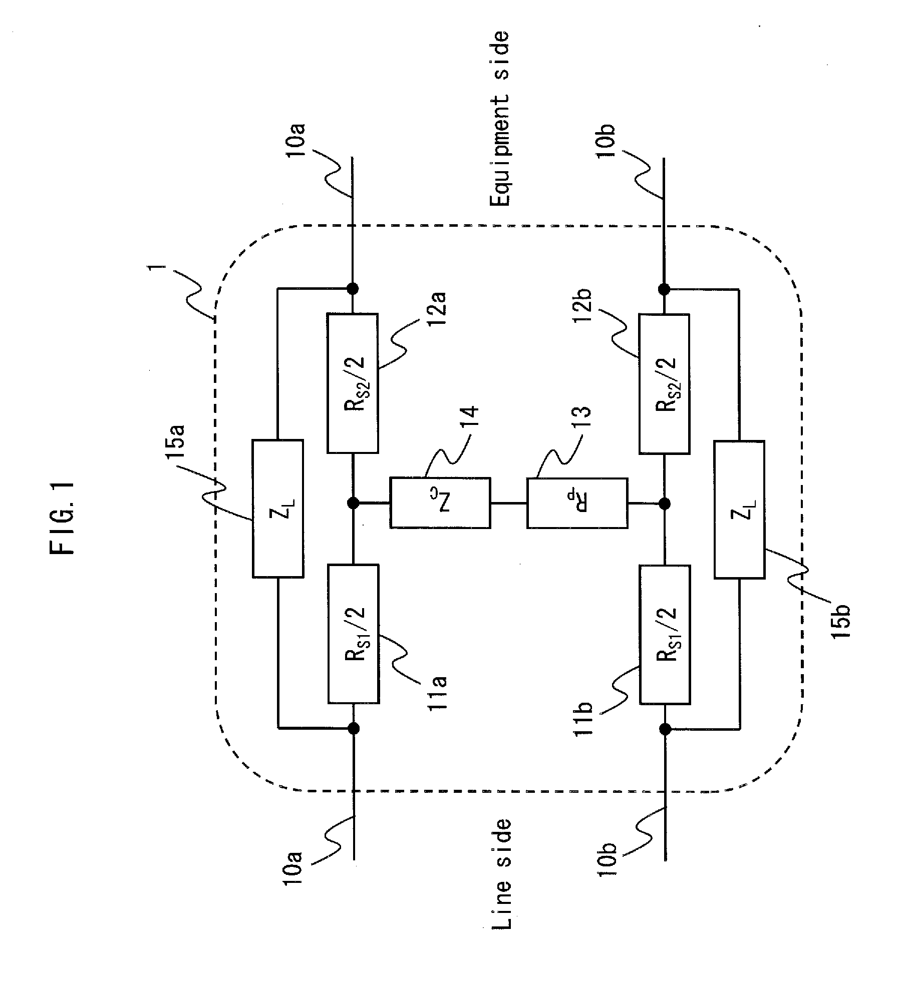
[0118]The impedance stabilization device 70 includes the series matching impedance elements 11a, 11b, 12a and 12b, the parallel matching impedance element 13, the low-frequency blocking element 14, and the high-frequency blocking elements 15a, 15b, 15c and 15d, as illustrated in FIG. 7A.
[0119]The impedance stabilization device 70 differs from the impedance stabilization device 1 in that each series matching impedance element is connected in parallel with a corr...
embodiment 2
Modification of Embodiment 2
[0153]The following describes various modifications of the impedance stabilization device 110 in Embodiment 2. Note that differences from the impedance stabilization device 110 are mainly described here.
modification 1
of Embodiment 2
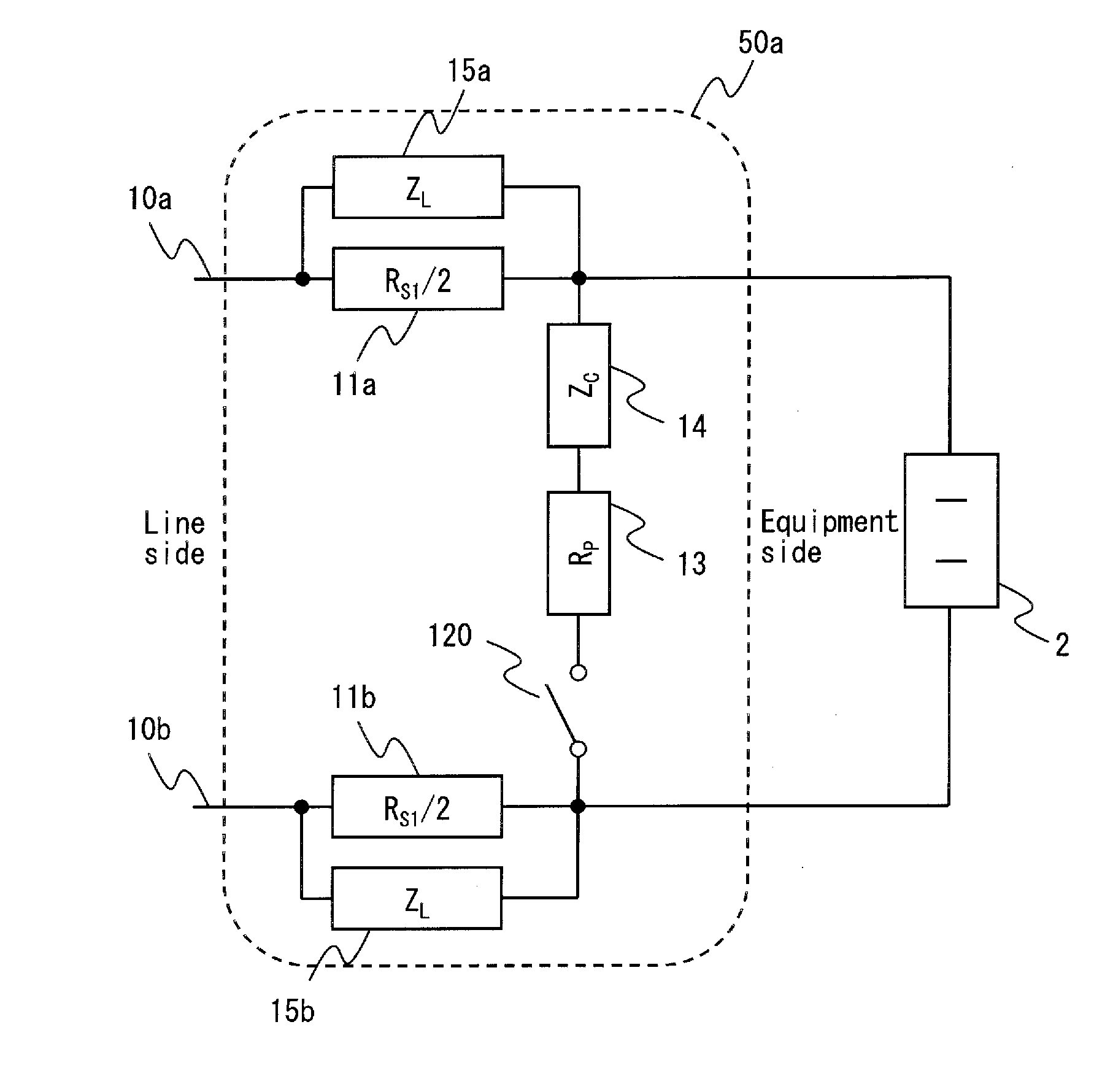
[0154]An impedance stabilization device 1300 illustrated in FIG. 13 differs from the impedance stabilization device 110 illustrated in FIG. 11 in that the matching impedance element 130 is removed, and the impedance upper circuit 160 is inserted at a side closer to not the socket connector 2 but the line than the switch 120 is. The impedance upper circuit 160 has the same configuration as that illustrated in FIG. 12. The total impedance of the two resistance elements 162a and 162b included in the impedance upper circuit 160 is set so as to be approximately equal to the characteristic impedance of the wiring. Since the two resistance elements 162a and 162b double as the matching impedance element 130 included in the impedance stabilization device 110 illustrated in FIG. 11, the matching impedance element 130 is removed, and thus the circuit is simplified.
PUM
 Abstract
Description
Claims
Application Information


