

Power amplifier
a power amplifier and amplifier technology, applied in the direction of gated amplifiers, amplifiers with semiconductor devices only, amplifiers with semiconductor devices, etc., can solve the problem that the switch that can turn the channel on only by applying gate voltage cannot be formed, and achieves the effect of reducing the minimum operating voltage, widening the degree of freedom in design, and reducing the impedance mismatch
- Summary
- Abstract
- Description
- Claims
- Application Information
AI Technical Summary
Benefits of technology
Problems solved by technology
Method used
Image

Examples
first embodiment
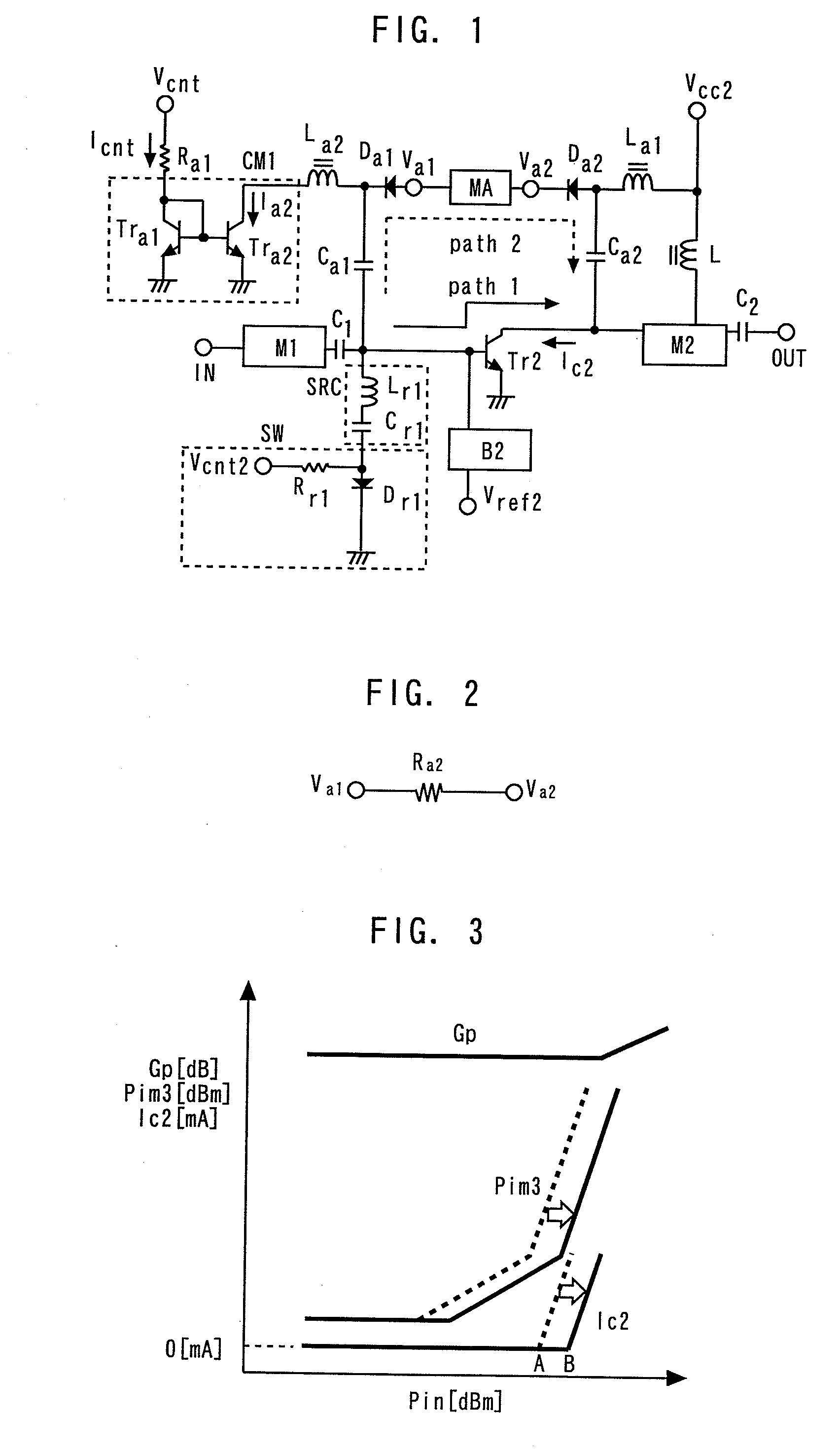
[0040]FIG. 1 is a circuit diagram showing a power amplifier according to a first embodiment of the present invention. The power amplifier is formed using a GaAs-HBT process.
[0041]The base of an amplifying transistor Tr2 that amplifies RF signals is connected to an input terminal IN via an input matching circuit M1 and a capacitor C1, the collector thereof is connected to an output terminal OUT via an output matching circuit M2 and a capacitor C2, and the emitter thereof is grounded. An inductor L is provided between a collector power terminal Vcc2 and the output matching circuit M2. A bias circuit B2 supplies bias current to the base of the amplifying transistor Tr2 corresponding to voltage applied to a control terminal Vref2.
[0042]The cathode of a BC diode Da1 (first diode) is connected to the input terminal IN via a capacitor Ca1 (first capacitor), the capacitor C1, and the input matching circuit M1. The anode of a BC diode Da2 (second diode) is connected to the output terminal OU...
second embodiment
[0059]FIG. 7 is a circuit diagram showing a power amplifier according to a second embodiment of the present invention. Components same as in the first embodiment are denoted by the same reference characters and numerals, and the description thereof will be omitted.
[0060]Other than the configuration of the switch SW, the second embodiment is identical to the first embodiment. The switch SW has a BC diode Dr1 (third diode), resistors Rr1 and Rr2, a current mirror circuit CM2 (second current mirror circuit), and a capacitor Cr2. The anode of the BC diode Dr1 is connected to a serial resonance circuit SRC. The resistor Rr2 is connected between the anode of the BC diode Dr1 and the power terminal Vcb2 of the bias circuit B2 (second power terminal). The current mirror circuit CM2 is connected to the cathode of the BC diode Dr1, and drives the BC diode Dr1.
[0061]The resistor Rr1 forms the reference current Icnt2 of the current mirror circuit CM2 corresponding to the voltage applied to the ...
third embodiment
[0064]FIG. 8 is a circuit diagram showing a power amplifier according to a third embodiment of the present invention. Components same as in the first or second embodiment are denoted by the same reference characters and numerals, and the description thereof will be omitted.
[0065]An inductor Lr1 (third inductor) and a capacitor Cr2 (third capacitor) are connected in series between a capacitor C1 and the base of an amplifying transistor Tr2. A capacitor Cr1 (fourth capacitor) is connected in parallel to the inductor Lr1. A switch SW is connected in parallel to the inductor Lr1, and connected in series to the capacitor Cr1.
[0066]The inductor Lr1 and the capacitor Cr2 compose a serial resonance circuit whose resonance frequency is set in the operating frequency band of the amplifying transistor Tr2. The inductor Lr1 and the capacitor Cr1 compose a parallel resonance circuit whose resonance frequency is set in the operating frequency band of the amplifying transistor Tr2.
[0067]The switch...
PUM
 Abstract
Description
Claims
Application Information