Liquid crystal display

a liquid crystal display and display technology, applied in the field of liquid crystal display, can solve the problems of large power consumption, data signal polarity needs to change on each data line, and large power consumption, and achieve the effect of reducing power consumption of lcd and good optical uniformity

Active Publication Date: 2012-04-19
BOE TECH GRP CO LTD
View PDF9 Cites 20 Cited by
  • Summary
  • Abstract
  • Description
  • Claims
  • Application Information

AI Technical Summary

Benefits of technology

[0011]According to the LCD provided by each embodiment of the disclosure, odd rows of pixel electrodes in the same column are controlled by one of the data lines at the two sides of the column, and even rows of pixel electrodes in the same column are controlled by the other one of the data lines at the two sides of the column; and two adjacent pixel electrodes in the same row between two adjacent data lines are respectively controlled by one of the two gate lines at the two sides of the row of pixel electrodes, and are respectively inputted with data signals by one of the two adjacent data lines. By that, the pixel electrodes that are inputted with data signals by the same data line are interleaved, and the polarity of any two adjacent pixel points is different, resulting in a good optical uniformity. Moreover, the polarity of signals output by each data line within one frame does not need to be changed, thus enabling reducing power consumption of LCD.

Problems solved by technology

For such LCD as shown in FIG. 1, if a good optical uniformity is required, the polarity of data signals on each data line needs to change constantly, and frequent change of the polarity of data signals leads to large power consumption.

Method used


Image

  • Liquid crystal display
  • Liquid crystal display
  • Liquid crystal display

Examples


first embodiment

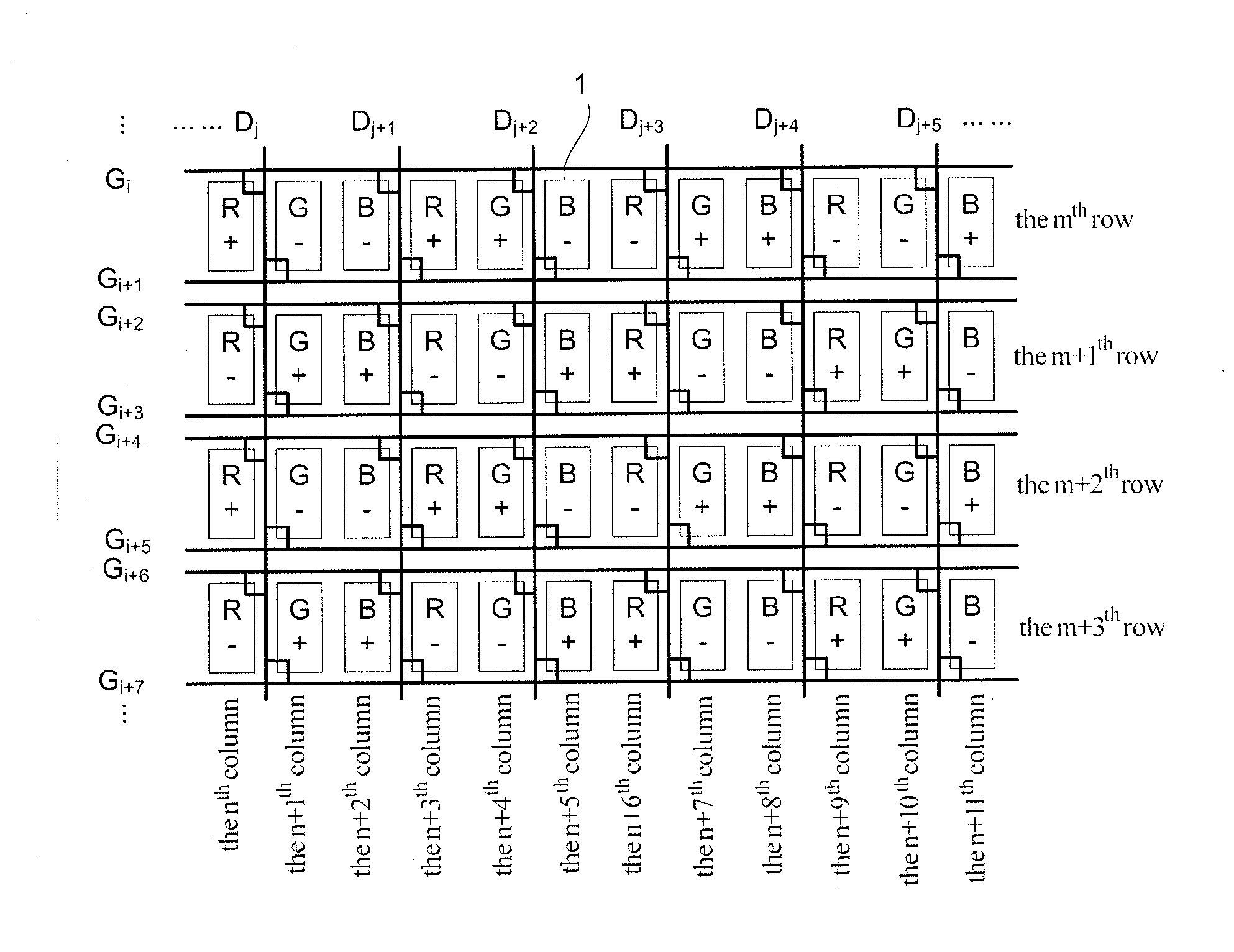
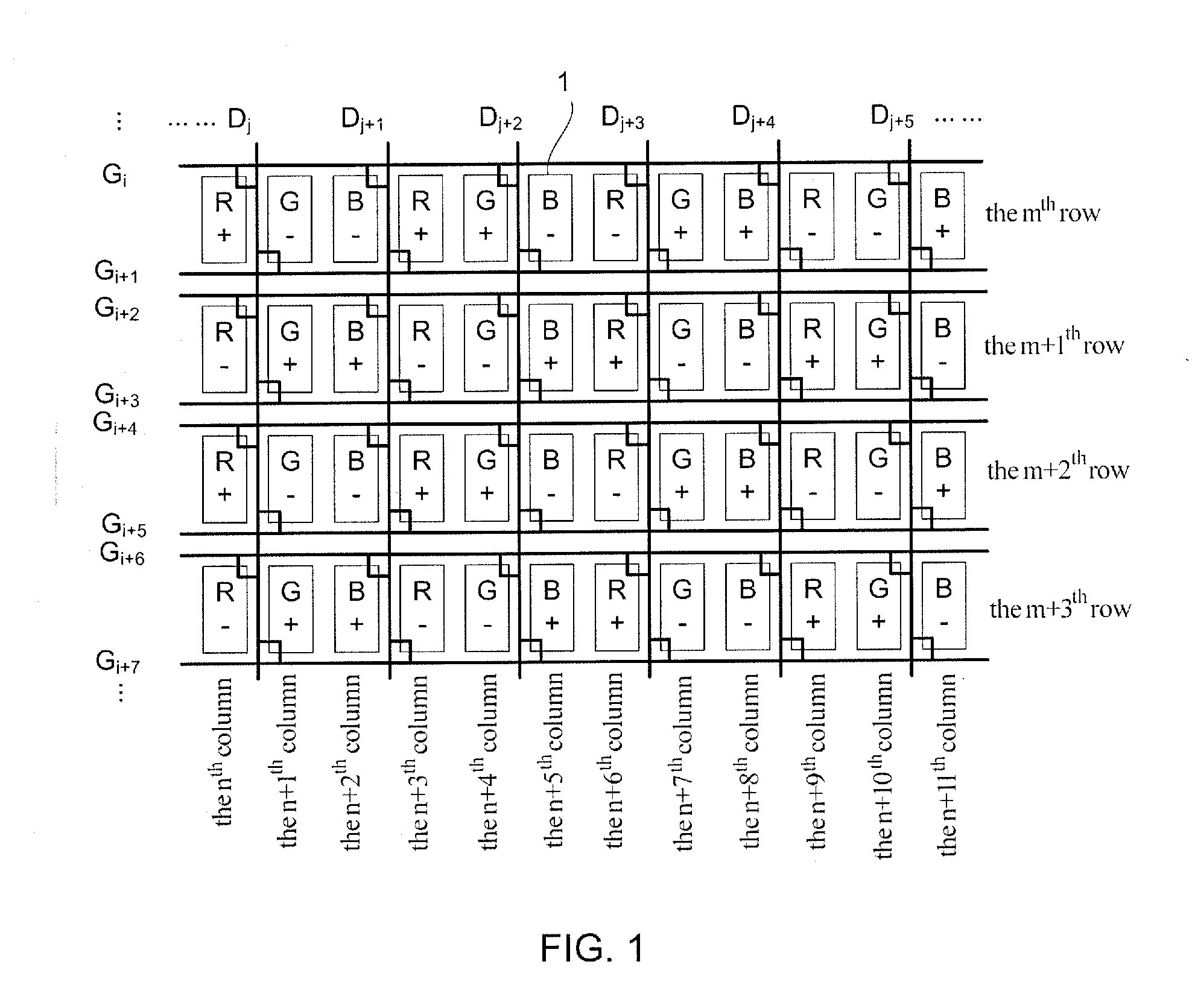
[0022]FIG. 3 schematically shows a structure of the LCD in the disclosure. The LCD includes an array substrate, on which there formed gate lines, data lines, and pixel electrodes 1. FIG. 3 shows a part of the array substrate, and the structure of the other part not shown is similar to that of the part shown. The gate lines shown in FIG. 3 are denoted with Gi, Gi+1, Gi+2, Gi+3, Gi+4, Gi+5, Gi+6, and Gi+7, respectively, and the data lines shown in FIG. 3 are denoted with Dj, Dj+1, Dj+2, Dj+3, Dj+4, and Dj+5, respectively. The pixel electrodes arranged in the vertical direction shown in FIG. 3 are referred to as the nth column of pixel electrodes (the pixel electrodes of column n), the n+1th column of pixel electrodes(the pixel electrodes of column n+1), the n+2th column of pixel electrodes (the pixel electrodes of column n+2), the n+3th column of pixel electrodes (the pixel electrodes of column n+3), the n+4th column of pixel electrodes (the pixel electrodes of column n+4), the n+5th ...

second embodiment

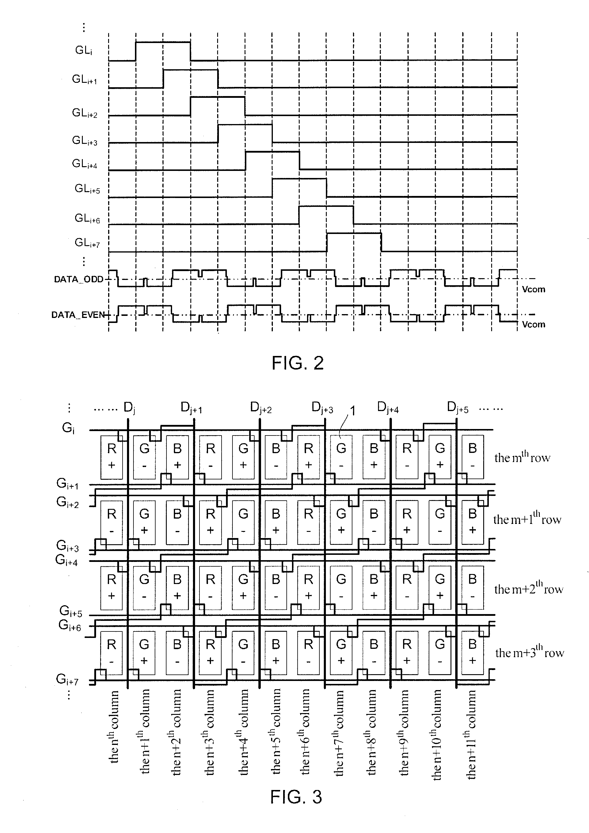
[0026]FIG. 4 shows a structural schematic diagram of the LCD of the present disclosure. A data line driving module 2 is added on the basis of the embodiment as shown in FIG. 3. The data line driving module 2 is respectively connected to each data line for inputting data signals with a first polarity into odd data lines, and inputting data signals with a second polarity into even data lines, during one frame; and inputting data signals with the second polarity into odd data lines, and inputting data signals with the first polarity into even data lines, during the next frame.

[0027]FIG. 5 and FIG. 6 are schematic diagrams of driving signals in the frame x and frame x+1 of the LCD of the present disclosure, respectively, wherein x is a natural number, and FIG. 7 is a schematic diagram of the LCD shown in FIG. 4 with the polarity of each pixel electrode inverted. Signals output by each gate line in FIG. 5 and FIG. 6 are the same as that in FIG. 2, and signals inputted on the common elect...

third embodiment

[0048]FIG. 8 is a structural schematic diagram of the LCD of the present disclosure. The LCD is configured such that among the pixel electrodes in the same column, two adjacent pixel electrodes are grouped into one group, the pixel electrodes in the odd groups are inputted with data signals by one of the data lines at two sides of the column of pixel electrodes, and the pixel electrodes in the even groups are inputted with data signals by the other one of the data lines at two sides of the column of pixel electrodes; the pixel electrodes in the same row are respectively controlled by one of the two gate lines at the two sides of the row of pixel electrodes, and the pixel electrodes controlled by each gate line are located in the same row; there are two gate lines between two adjacent rows of pixel electrodes; two adjacent pixel electrodes in the same row between two adjacent data lines are respectively controlled by one of the two gate lines at the two sides of the row of pixel elec...


PUM


Abstract

A liquid crystal display comprising an array substrate formed with gate lines, data lines and pixel electrodes. Odd rows of pixel electrodes in the same column are connected with one of data lines at two sides of the column, even rows of pixel electrodes are connected with the other one of the data lines; pixel electrodes in the same row are controlled by one of the two gate lines at two sides of the row of pixel electrodes, pixel electrodes controlled by each gate line are located in the same row; there are two gate lines between two adjacent rows of pixel electrodes; two adjacent pixel electrodes in the same row between two adjacent data lines are controlled by one of the two gate lines at two sides of the row of pixel electrodes, and they are connected with one of the two adjacent data lines.

Description

TECHNICAL FIELD[0001]The present disclosure relates to a technology of liquid crystal display (LCD), and in particular, relates to a LCD.RELATED ART[0002]FIG. 1 shows a schematic structure of an array substrate of a LCD in the related art, in which the array substrate includes gate lines, data lines and pixel electrodes 1. A part of the array substrate is shown in FIG. 1, and the structure of the part not shown is similar to that of the part shown. The gate lines shown in FIG. 1 are denoted with Gi, Gi+1, Gi+2, Gi+3, Gi+4, Gi+5, Gi+6, and Gi+7, respectively, and the data lines shown in FIG. 1 are denoted with Dj, Dj+1, Dj+2, Dj+3, Dj+4, and Dj+5, respectively.[0003]In the structure shown in FIG. 1, two adjacent columns of pixel electrodes are input with data signals by the same data line. In the same row, two pixel electrodes 1 connected with the same data line are each controlled by one of the two gate lines at the two sides of the row of pixel electrodes 1. By the array substrate ...

Claims


Application Information

Patent Timeline
Patent Type & Authority Applications(United States)
IPC IPC(8): G09G3/36
CPCG09G3/3614G09G3/3648G09G2330/021G09G2310/0205G09G2300/0426G02F1/133G09G3/36
Inventor SHANG, GUANGLIANG
Owner BOE TECH GRP CO LTD
Why Eureka
Try Eureka